物料型号:PJM2302NSC
器件简介:N-增强型模式场效应晶体管
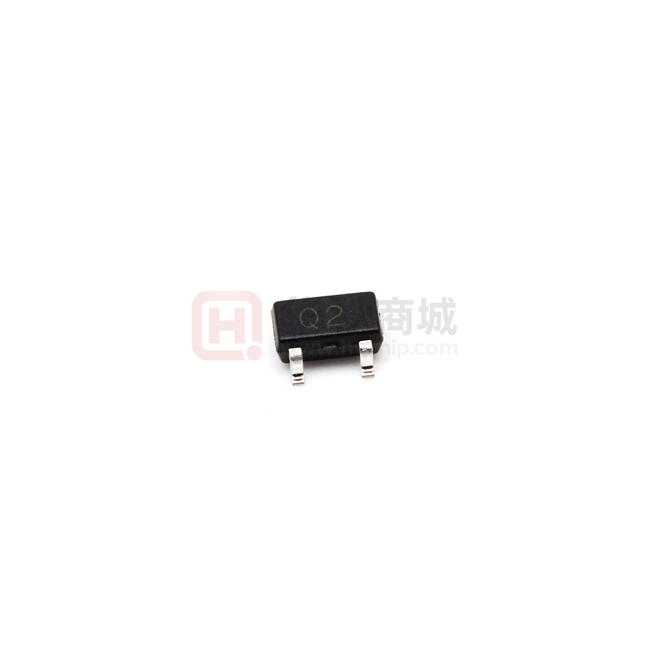
封装类型:SOT-23-3
引脚分配:
1. Gate(栅极)
2. Source(源极)
3. Drain(漏极)
标记:Q2
参数特性:
- 漏源电压(VDS)= 20V
- 漏极电流(ID)= 4A
- 在VGS=2.5V时,RDS(ON) < 55mΩ
- 在VGS=4.5V时,RDS(ON) < 40mΩ
- 低栅极电荷和RDS(on),高功率和电流处理能力
功能详解:
- 适用于负载开关和PWM应用
- 电源管理
应用信息:
- 负载开关和PWM应用
- 电源管理
封装信息:
- 封装类型:SOT-23-3
- 尺寸(单位:mm):2.92 x 2.8 x 1.27
- 订购信息:每卷3000个,带7英寸卷轴
绝对最大额定值:
- 漏源电压(VDs):20V
- 栅源电压(VGs):±12V
- 连续漏极电流(ID):4A
- 脉冲漏极电流(IoM):20A
- 最大功率耗散(PD):1.25W
- 工作结和存储温度范围(TJ,TSTG):-55至150°C
热特性:
- 结到环境的热阻(RBJA):100°C/W
电气特性:
- 静态特性包括漏源击穿电压、零栅极电压漏极电流、栅体漏电流、栅极阈值电压和漏源导通电阻等。
- 动态特性包括输入电容、输出电容和反向传输电容。
- 开关特性包括开通延迟时间、开通上升时间、关断延迟时间和关断下降时间。
典型特性曲线:
- 提供了关于开关测试电路、开关波形、功率耗散、漏极电流、输出特性和漏源导通电阻的图表。
订购和存储条件:
- 推荐回流焊接条件、手工焊接条件和存储条件。
封装规格:
- 提供了胶带和卷轴数据,包括卷轴尺寸和胶带尺寸。