PJM60H12MNSA
N- Channel Depletion Mode MOSFETS
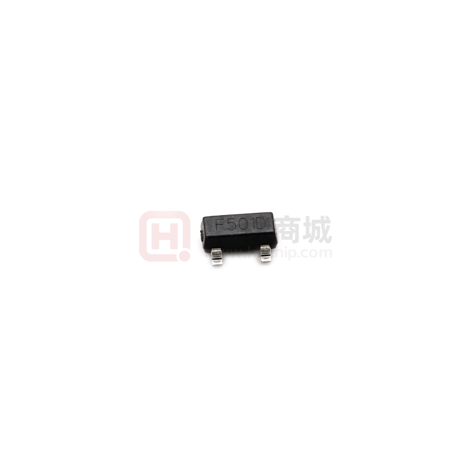
SOT-23
Features
⚫ Halogen and Antimony Free
⚫ Depletion Mode
⚫ ESD improved Capability
⚫ VDS= 600V,ID= 0.03A
RDS(on)< 800Ω @VGS= 10V
1. Gate
2.Source
3.Drain
Marking Code:F501D
Schematic Diagram
3.Drain
1.Gate
2.Source
Absolute Maximum Ratings
Ratings at 25℃ ambient temperature unless otherwise specified.
Parameter
Symbol
Value
Unit
Drain-Source Voltage
VDS
600
V
Gate-Source Voltage
VGS
±20
V
Drain Current-Continuous
ID
0.03
A
Drain Current-Pulsed
IDM
0.12
A
Maximum Power Dissipation
PD
0.5
W
VESD(G-S)
300
V
TJ
150
°C
TSTG
-55 to +150
°C
RθJA
250
℃/W
Gate Source ESD (HBM-C=100pF, R=1.5kΩ)
Junction Temperature
Storage Temperature Range
Thermal Characteristics
Thermal Resistance,Junction-to-Ambient
www.pingjingsemi.com
Revision:2.0 Jul-2021
1/7
�PJM60H12MNSA
N- Channel Depletion Mode MOSFETS
Electrical Characteristics
(Ta=25℃ unless otherwise specified)
Parameter
Symbol
Test Condition
Min.
Typ.
Max.
Unit
V(BR)DSS
VGS=-5V,ID=250μA
600
--
--
V
VDS=600V, VGS=-5V
--
--
0.1
μA
--
--
10
μA
OFF Characteristics
Drain-Source Breakdown Voltage
Gate-Body Leakage Current
ID(off)
VDS=480V, VGS=-5V,
TA=125°C
Gate Leakage Current
IGSS
VGS=±10V
--
--
±100
nA
VGS(off)
VDS=3V,ID=8μA
-2.7
-1.8
-1
V
IDSS
VGS=0V, VDS=25V
12
--
--
mA
VGS=0V, ID=3mA
--
350
700
Ω
VGS=10V, ID=16mA
--
400
800
Ω
VDS=50V,ID=0.01A
8
17
--
mS
--
50
--
pF
--
4.53
--
pF
ON Characteristics
Gate-to-Source Cut-off Voltage
On-State Drain Current
Drain-Source On-Resistance
RDS(on)
Dynamic Characteristics
Forward Transconductance
gFS
Input Capacitance
Ciss
Output Capacitance
Coss
Reverse Transfer Capacitance
Crss
--
1.08
--
pF
Turn-on Delay Time
td(on)
--
9.9
--
nS
Turn-on Rise Time
tr
VDD=300V, ID=0.01A
--
55.8
--
nS
Turn-off Delay Time
td(off)
VGS=-5V~7V,RG=6Ω
--
56.4
--
nS
--
136
--
nS
--
1.14
--
nC
--
0.5
--
nC
--
0.37
--
nC
--
--
1.2
V
--
--
0.025
A
--
0.75
1.2
V
VDS=25V,VGS=-5V,f=1MHz
Switching Characteristics
Turn-off Fall Time
tf
Total Gate Charge
Qg
Gate-Source Charge
Qgs
Gate-Drain Charge
Qgd
VDD=400V,ID=0.01A,
VGS=-5V~5V
Drain-Source Diode Characteristics
Diode Forward Voltage
VSD
Diode Forward Current
IS
VGS=-5V,IF=16mA
Gate-Source Zener Diode
Gate-Source Breakdown Voltage
www.pingjingsemi.com
Revision:2.0 Jul-2021
VGSO
IGS=±1mA (Open Drain)
2/7
�PJM60H12MNSA
N- Channel Depletion Mode MOSFETS
Typical Characteristic Curves
1.15
Normalized Breakdown Voltage
Normalized On-Resistance
2.25
2.00
1.75
1.30
1.25
1.00
0.75
0.50
-75
1.10
1.05
1.00
0.95
0.90
-50
-25
-0
25
50
75
100
125
150
-75
-50
-25
TJ Junction Temperature (℃)
0
25
50
75
100
125
150
TJ Junction Temperature (℃)
C Capacitance (pF)
Ciss
Coss
Crss
VGS=-5V, f=1MHz
Ciss=Cgs+Cgd
Coss=Cds=Cgd
Crss=Cgd
VGS Gate-Source Voltage (V)
+5
VDS=100V
VDS=250V
+3
VDS=400V
+1
-1
-3
-5
VDS Drain-Source Voltage (V)
0
0.2
0.4
0.6
0.8
1.0
1.2
Qg Total Gate Charge (nC)
0.025
1ms
10ms
100ms
DC
Operation in This Area May be
Limited by RDS(on)
TJ=Max Rated TC=25℃
0.020
ID Drain Current (A)
ID Drain Current (A)
100μs
0.015
0.010
0.005
0.000
VDS Drain-Source Voltage (V)
www.pingjingsemi.com
Revision:2.0 Jul-2021
0
3
6
9
12
15
VDS Drain-Source Voltage (V)
3/7
�PJM60H12MNSA
N- Channel Depletion Mode MOSFETS
IDM Peak Drain Current (A)
100
For Temperatures
Above 25℃ Derate Peak
Current as Follows
Transconductance may
Limited in This Region
10
1
1.00E-05
1.00E-03
1.00E-04
1.00E-02
1.00E+01
1.00E+00
1.00E-01
t Pulse Width (s)
6
9
ID Drain Current (A)
7.5
RDS(on) On-Resistance (Ω)
Pulse Duration=10μs
Duty Factor=0.5%Max
VDS=30V
6
4.5
-55℃
3
+25℃
1.5
0
150℃
2
3
4
5
5
4
ID=4A
ID=2A
3
ID=1A
2
1
0
6
Pulse Duration=10μs
Duty Factor=0.5%Max
TC=25℃
4
VGS Gate-Source Voltage (V)
10
12
14
2.50
Pulse Duration=10μs
Duty Factor=0.5%Max
TC=25℃
Normalized Breakdown Voltage
RDS(on) On-Resistance (Ω)
8
VGS Gate-Source Voltage (V)
3
2.5
2
VGS=20V
1.5
1
6
0
www.pingjingsemi.com
Revision:2.0 Jul-2021
1
2
3
ID Drain Current (A)
4
2.25
2.00
Pulse Duration=10μs
Duty Factor=0.5%Max
VGS=10V, ID=2A
1.75
1.50
1.25
1.00
0.75
0.5
-50
0
50
100
150
TJ Junction Temperature (℃)
4/7
�PJM60H12MNSA
N- Channel Depletion Mode MOSFETS
Package Outline
SOT-23
Dimensions in mm
Ordering Information
Device
Package
Shipping
PJM60H12MNSA
SOT-23
3,000PCS/Reel&7inches
www.pingjingsemi.com
Revision:2.0 Jul-2021
5/7
�PJM60H12MNSA
N- Channel Depletion Mode MOSFETS
Conditions of Soldering and Storage
Recommended condition of reflow soldering
Recommended peak temperature is over 245 OC. If peak temperature is below 245 OC, you may adjust
the following parameters:
Time length of peak temperature (longer)
Time length of soldering (longer)
Thickness of solder paste (thicker)
Conditions of hand soldering
Temperature: 370 OC
Time: 3s max.
Times: one time
Storage conditions
Temperature
5 to 40 OC
Humidity
30 to 80% RH
Recommended period
One year after manufacturing
www.pingjingsemi.com
Revision:2.0 Jul-2021
6/7
�PJM60H12MNSA
N- Channel Depletion Mode MOSFETS
Package Specifications
The method of packaging
Cover Tape
3,000 pcs per reel
SOT-23
Carrier Tape
30,000 pcs per box
10 reels per box
120,000 pcs per carton
4 boxes per carton
Embossed tape and reel data
D
A
T2
T1
Symbol
A
B
C
E
F
D
T1
T2
B
C
E
Value (unit: mm)
Ø 177.8±1
2.7±0.2
Ø 13.5±0.2
Ø 54.5±0.2
12.3±0.3
9.6+2/-0.3
1.0±0.2
1.2±0.2
F
Reel (7'')
www.pingjingsemi.com
Revision:2.0 Jul-2021
7/7
�
很抱歉,暂时无法提供与“PJM60H12MNSA”相匹配的价格&库存,您可以联系我们找货
免费人工找货- 国内价格
- 10+0.42066
- 100+0.33254
- 300+0.28847
- 国内价格
- 5+0.26386
- 20+0.24016
- 100+0.21646
- 500+0.19276
- 1000+0.18170
- 2000+0.17380