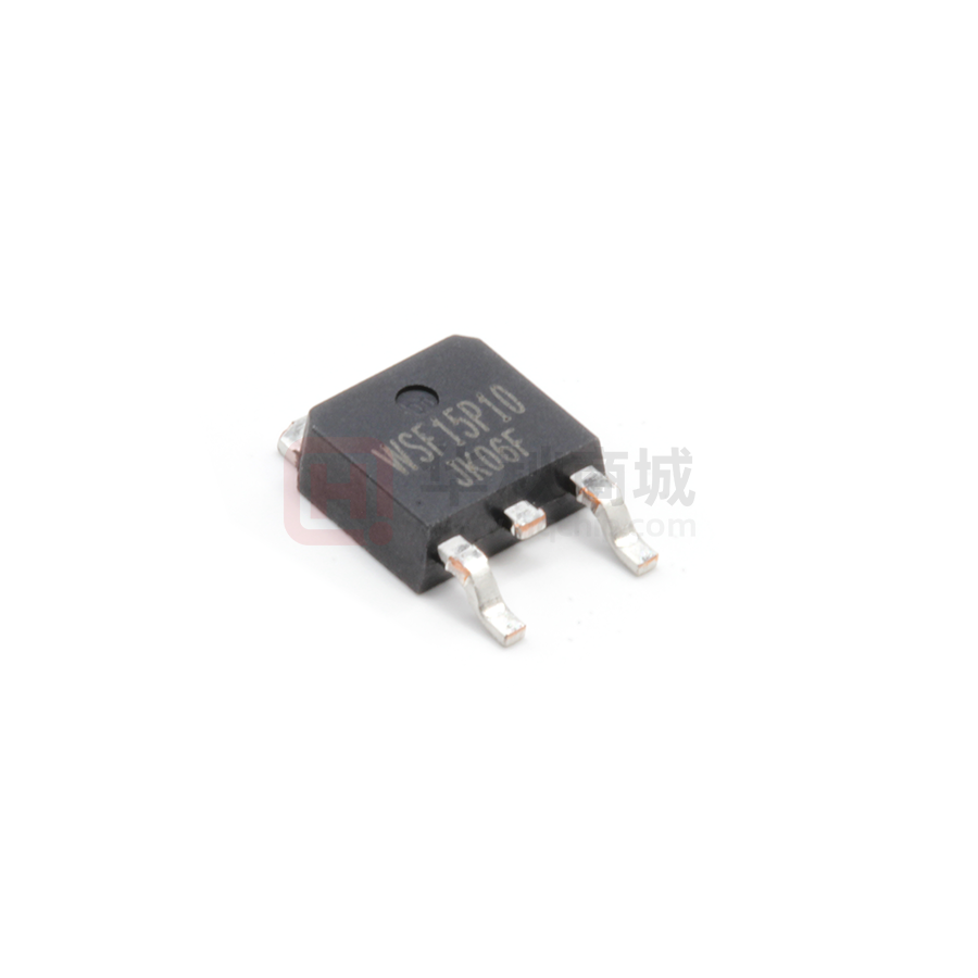
WSF15P10
P-Ch MOSFET
Product Summery
General Description
The WSF15P10 is the highest performance trench
P-ch MOSFET with extreme high cell density ,
which provide excellent RDSON and gate charge
for most of the synchronous buck converter
applications .
BVDSS
RDSON
ID
-100V
150mΩ
-13A
Applications
The WSF15P10 meet the RoHS and Green
Product requirement,100% EAS guaranteed with
full function reliability approved.
z High Frequency Point-of-Load Synchronous
Buck Converter for MB/NB/UMPC/VGA
z Networking DC-DC Power System
Features
z Load Switch
z Advanced high cell density Trench technology
TO-252 Pin Configuration
z Super Low Gate Charge
z Excellent CdV/dt effect decline
z 100% EAS Guaranteed
z Green Device Available
Absolute Maximum Ratings
Symbol
Parameter
VDS
VGS
ID@TC=25℃
ID@TC=100℃
IDM
Rating
Units
Drain-Source Voltage
-100
V
Gate-Source Voltage
±20
V
1
-13
A
1
-7
A
-45
A
Continuous Drain Current, -VGS @ -10V
Continuous Drain Current, -VGS @ -10V
Pulsed Drain Current
2
EAS
Single Pulse Avalanche Energy
25
mJ
IAS
Avalanche Current
-10
A
3
4
PD@TC=25℃
Total Power Dissipation
50
W
TSTG
Storage Temperature Range
-55 to 150
℃
TJ
Operating Junction Temperature Range
-55 to 150
℃
Thermal Data
Symbol
Parameter
Max.
Unit
RθJA
Thermal Resistance Junction-Ambient 1
---
50
℃/W
RθJC
Thermal Resistance Junction-Case1
---
2.5
℃/W
www.winsok.tw
Typ.
Page 1
Dec.2016
�WSF15P10
P-Ch MOSFET
Electrical Characteristics (TJ=25 ℃, unless otherwise noted)
Symbol
BVDSS
Parameter
Conditions
Drain-Source Breakdown Voltage
△BVDSS/△TJ BVDSS Temperature Coefficient
RDS(ON)
VGS(th)
2
Static Drain-Source On-Resistance
Gate Threshold Voltage
Min.
Typ.
Max.
Unit
VGS=0V , ID=-250uA
-100
---
---
V
Reference to 25℃ , ID=-1mA
---
-0.021
---
V/℃
VGS=-10V , ID=-5.5A
---
150
205
mΩ
-1
---
-3
V
---
4.08
---
mV/℃
VDS=-48V , VGS=0V , TJ=25℃
---
---
1
VDS=-48V , VGS=0V , TJ=55℃
---
---
5
VGS=VDS , ID =-250uA
△VGS(th)
VGS(th) Temperature Coefficient
IDSS
Drain-Source Leakage Current
IGSS
Gate-Source Leakage Current
VGS=±20V , VDS=0V
---
---
±100
nA
gfs
Forward Transconductance
VDS=-10V , ID=-6A
---
8
---
S
Qg
Total Gate Charge (-4.5V)
---
21
---
Qgs
Gate-Source Charge
---
4.3
---
Qgd
Gate-Drain Charge
---
5.2
---
Turn-On Delay Time
---
11
23
Td(on)
Tr
Td(off)
Tf
VDS=-50V , VGS=-10V , ID=-5.5A
uA
nC
Rise Time
VDD=-30V , VGS=-10V , RG=6Ω,
---
10
20
Turn-Off Delay Time
ID=-1A ,RG=30Ω.
---
55
120
---
30
65
---
1050
---
---
70
---
---
30
---
Min.
Typ.
Max.
Unit
20
---
---
mJ
Min.
Typ.
Max.
Unit
A
Fall Time
Ciss
Input Capacitance
Coss
Output Capacitance
Crss
Reverse Transfer Capacitance
VDS=-30V , VGS=0V , f=1MHz
ns
pF
Guaranteed Avalanche Characteristics
Symbol
EAS
Parameter
Conditions
5
Single Pulse Avalanche Energy
VDD=-25V , L=0.5mH , IAS=-10A
Diode Characteristics
Symbol
Parameter
Conditions
1,6
IS
Continuous Source Current
ISM
Pulsed Source Current
VSD
Diode Forward Voltage2
2,6
VG=VD=0V , Force Current
VGS=0V , IS=-1A , TJ=25℃
---
---
-2.0
---
---
-45
A
---
---
-1.2
V
Note :
1.The data tested by surface mounted on a 1 inch2 FR-4 board with 2OZ copper,t≦10sec.
2.The data tested by pulsed , pulse width ≦ 300us , duty cycle ≦ 2%
3.The EAS data shows Max. rating . The test condition is VDD=-25V,VGS=-10V,L=0.5mH,IAS=-10A
4.The power dissipation is limited by 150℃ junction temperature
5.The Min. value is 100% EAS tested guarantee.
6.The data is theoretically the same as ID and IDM , in real applications , should be limited by total power dissipation.
www.winsok.tw
Page 2
Dec.2016
�WSF15P10
P-Ch MOSFET
Typical Characteristics
210
8
ID=-5.5A
-ID Drain Current (A)
6
190
RDSON (mΩ)
VGS=-10V
VGS=-7V
VGS=-5V
4
VGS=-4.5V
2
170
160
VGS=-3V
0
0
0.5
1
1.5
-VDS , Drain-to-Source Voltage (V)
130
2
2
Fig.1 Typical Output Characteristics
4
6
-VGS (V)
8
10
Fig.2 On-Resistance v.s Gate-Source
6
10
-VGS Gate to Source Voltage (V)
IS Source Current(A)
VDS=-50V
4
TJ=150℃
TJ=25℃
2
0
0.0
0.4
0.8
ID=-5.5A
8
6
4
2
0
0
1.2
Fig.3 Forward Characteristics Of Reverse
5
7.5
10
Fig.4 Gate-Charge Characteristics
2.0
Normalized On Resistance
1.5
Normalized VGS(th)
2.5
QG , Total Gate Charge (nC)
VSD , Source-to-Drain Voltage (V)
1.5
1
1.0
0.5
0.5
0
-50
0
50
100
TJ ,Junction Temperature ( ℃)
-50
150
Fig.5 Normalized VGS(th) v.s TJ
www.winsok.tw
0
50
100
150
TJ , Junction Temperature (℃)
Fig.6 Normalized RDSON v.s TJ
Page 3
Dec.2016
�WSF15P10
P-Ch MOSFET
Capacitance (pF)
10000
100
F=1.0MHz
10us
1000
10
100us
-ID (A)
Ciss
1
100
10ms
100ms
Coss
DC
TC=25℃
Single Pulse
Crss
0
10
1
5
9
13
17
21
-VDS Drain to Source Voltage(V)
0.1
25
1
Fig.7 Capacitance
10
100
-VDS (V)
1000
Fig.8 Safe Operating Area
Normalized Thermal Response (RθJC)
1
DUTY=0.5
0.2
0.1
0.1
0.05
P DM
T ON
0.02
0.01
T
D = TON/T
TJpeak = TC+P DMXRθJC
SINGLE
0.01
0.00001
0.0001
0.001
0.01
0.1
1
t , Pulse Width (s)
Fig.9 Normalized Maximum Transient Thermal Impedance
Fig.10 Switching Time Waveform
www.winsok.tw
Fig.11 Unclamped Inductive Waveform
Page 4
Dec.2016
�Attention�
1,�Any�and�all�Winsok�power�products�described�or�contained�herein�do�not�have�specifications�that�can�handle�
applications�that�require�extremely�high�levels�of�reliability,�such�as�lifeͲsupport�systems,�aircraft's�control�systems,�or�
other�applications�whose�failure�can�be�reasonably�expected�to�result�in�serious�physical�and/or�material�damage.� �
Consult�with�your�Winsok�power�representative�nearest�you�before�using�any�Winsok�power�products�described�or�
contained�herein�in�such�applications.�
2,Winsok�power�assumes�no�responsibility�for�equipment�failures�that�result�from�using�products�at�values�that�exceed,� �
even�momentarily,�rated�values�(such�as�maximum�ratings,�operating�condition�ranges,�or�other�parameters)�listed�in�
products�specifications�of�any�and�all�Winsok�power�products�described�or�contained�herein.�
3,�Specifications�of�any�and�all�Winsok�power�products�described�or�contained�herein�stipulate�the�performance,�
characteristics,�and�functions�of�the�described�products�in�the�independent�state,�and�are�not�guarantees�of�the�
performance,�characteristics,�and�functions�of�the�described�products�as�mounted�in�the�customer’s�products�or�
equipment.�To�verify�symptoms�and�states�that�cannot�be�evaluated�in�an�independent�device,�the�customer�should�always�
evaluate�and�test�devices�mounted�in�the�customer’s�products�or�equipment.�
4,�Winsok�power�Semiconductor�CO.,�LTD.�strives�to�supply�highͲquality�highͲreliability�products.�However,�any�and�all�
semiconductor�products�fail�with�some�probability.�It�is�possible�that�these�probabilistic�failures�could�give�rise�to�accidents�
or�events�that�could�endanger�human�lives�that�could�give�rise�to�smoke�or�fire,�or�that�could�cause�damage�to�other�
property.�When�designing�equipment,�adopt�safety�measures�so�that�these�kinds�of�accidents�or�events�cannot�occur.�Such�
measures�include�but�are�not�limited�to�protective�circuits�and�error�prevention�circuits�for�safe�design,�redundant�design,�
and�structural�design.�
5,In�the�event�that�any�or�all�Winsok�power�products(including�technical�data,�services)�described�or�contained�herein�are�
controlled�under�any�of�applicable�local�export�control�laws�and�regulations,�such�products�must�not�be�exported�without�
obtaining�the�export�license�from�the�authorities�concerned�in�accordance�with�the�above�law.�
6,�No�part�of�this�publication�may�be�reproduced�or�transmitted�in�any�form�or�by�any�means,�electronic�or�mechanical,�
including�photocopying�and�recording,�or�any�information�storage�or�retrieval�system,�or�otherwise,�without�the�prior�
written�permission�of�Winsok�power�Semiconductor�CO.,�LTD.�
7,�Information�(including�circuit�diagrams�and�circuit�parameters)�herein�is�for�example�only;�it�is�not�guaranteed�for�
volume�production. Winsok�power�believes�information�herein�is�accurate�and�reliable,�but�no�guarantees�are�made�or�
implied�regarding�its�use�or�any�infringements�of�intellectual�property�rights�or�other�rights�of�third�parties.�
8,�Any�and�all�information�described�or�contained�herein�are�subject�to�change�without�notice�due�to�product/technology�
improvement,etc.�When�designing�equipment,�refer�to�the�"Delivery�Specification"�for�the�Winsok�power�product�that�you� �
Intend�to�use.�
9,�this�catalog�provides�information�as�of�Sep.2014. Specifications�and�information�herein�are�subject�to�change�without�
notice.�
�