WPM2341
WPM2341
P-Channel Enhancement Mode Mosfet
Http://www.sh-willsemi.com
Features
z� Higher Efficiency Extending Battery Life
z� Miniature SOT23-3 Surface Mount Package
z� Super high density cell design for extremely low RDS (ON)
3
1
Applications
2
z�DC/DC Converter
z�Load Switch
z�Battery Powered System
z�
z�LCD Display inverter
z�Power Management in Portable, Battery Powered Products
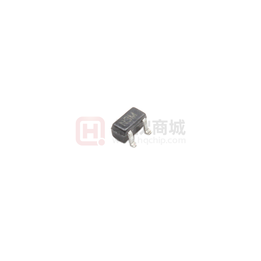
SOT 23-3
pin connections :
PïChannel
ABSOLUTE MAXIMUM RATINGS TA = 25 °C, unless otherwise noted
Steady
Parameter
Symbol
Drain-Source Voltage
VDS
-20
Gate-Source Voltage
VGS
±8
Continuous Drain Current
a
(TJ = 150 °C)
TA=25°C
TA=80°C
Pulsed Drain Current
IS
(Diode Conduction) a
Dissipation
a
TA=25°C
TA=80°C
Operating Junction and Storage
Temperature Range
PD
State
Unit
-3.5
-3.2
-2.5
G
1
3
S
V
-4.3
IDM
Continuous Source Current
Maximum Power
ID
5s
2
Top View
Marking:
A
-20
-1.7
-1
1.25
0.75
0.7
0.42
Drain
3
W41Z
W
2
1
TJ, Tstg
- 55 to 150
D
°C
Gate
Source
W 41= Specific Device Code
a. Surface Mounted on FR4 Board using 1 in sq pad size,2oz Cu.
Z = Date Code
Order information
Part�Number�
Package�
WPM2341Ͳ3/TR
�
SOT23-3
Will Semiconductor Ltd.
Shipping� �
�
1
3000�Tape�&�Reel�
2015/08/25 – Rev. 1.9
�WPM2341
THERMAL RESISTANCE RATINGS ��
Parameter
Junction-to-Ambient Thermal Resistance b
Symbol
t5s
Steady State
Typical
Maximum
75
100
125
165
RșJA
Unit
°C/W
b. Surface Mounted on FR4 Board using 1 in sq pad size, 2oz Cu.
MOSFET ELECTRICAL CHARACTERISTICS(TJ =25 ć unless otherwise specified)
Parameter
Symbol
Test Condition
Off Characteristics
Drain-Source Breakdown Voltage
BVDSS
VGS = 0V,ID = -250ȝA
Zero Gate Voltage Drain Current
IDSS
VDS =-16V,VGS = 0V
Gate –Source leakage current
IGSS
VGS = f8 V,VDS = 0V
On Characteristics
Gate Threshold Voltage
VGS(th)
VGS = VDS, ID =-250ȝA
Static Drain-Source
VGS = -4.5V, ID = -3.3A
RDS(on)
On-Resistance
VGS = -2.5V,ID = -2.8 A
Forward Transconductance
gFS
VDS = -5 V, ID = -3.3A
Dynamic Characteristics
Input Capacitance
Ciss
VDS = -6 V, VGS = 0V,
Output Capacitance
Coss
f = 1.0 MHz
Reverse Transfer Capacitance
Crss
Switching Characteristics
Turn-On Delay Time
td(on)
Turn-On Rise Time
tr
VGS = -4.5V, VDD = -6 V,
ID = -1.0A, RG=6.0ȍ,
Turn-Off Delay Time
td(off)
Turn-Off Fall Time
tf
Total Gate Charge
QG(TOT)
Threshold gate charge
QG(TH)
VDS = -6 V,I D = -3.3A,
VGS =-4.5V
Gate-Source Charge
QGS
Gate-Drain Charge
QGD
Drain-Source Diode Characteristics and Maximun Ratings
Forward Diode Voltage
VSD
VGS = 0V,IS = -1.6A
Will Semiconductor Ltd.
2
Min
Typ
Max
Units
-1
f100
V
ȝA
nA
-20
-0.35
-0.63
52
65
3.0
8
0.2
1.2
2.2
-0.8
-1.00
61
71
V
mȍ
mȍ
S
700
160
120
pF
pF
pF
25
55
90
60
13
ns
ns
ns
ns
nC
nC
nC
nC
V
2015/08/25 – Rev. 1.9
�WPM2341
Typical Characteristics
(TJ = 25°C unless otherwise noted)
20
20
VGS =-5 thru -2.5 V
16
-2 V
-I D - Drain Current (A)
-I D - Drain Current (A)
16
TC = - 55 °C
12
8
-1.5 V
4
25 °C
125 °C
12
8
4
-1 V
0
0
1
2
3
4
0
0.0
5
0.5
-VDS - Drain-to-Source Voltage (V)
1.5
2.0
2.5
-V GS - Gate-to-Source Voltage (V)
Output Characteristics
Transfer Characteristics
900
0.10
750
0.08
VGS =-2.5 V
C - Capacitance (pF)
R DS(on) - On-Resistance (Ω)
1.0
0.06
0.04
VGS =-4.5 V
600
Ciss
450
300
0.02
150
Coss
Crss
0
0.00
0
4
8
12
16
0
20
8
12
16
-I D - Drain Current (A)
-VDS - Drain-to-Source Voltage (V)
On-Resistance vs. Drain Current
Capacitance
20
1.5
5
1.4
VDS =-6 V
ID =-3.3 A
1.3
3
2
1
VGS =-4.5 V
ID =-3.3 A
1.2
(Normalized)
4
R DS(on) - On-Resistance
-VGS - Gate-to-Source Voltage (V)
4
1.1
1.0
0.9
0.8
0.7
0.6
- 50
0
0
2
4
6
8
10
- 25
0
25
50
75
100
125
Qg - Total Gate Charge (nC)
TJ - Junction Temperature (°C)
Gate Charge
On-Resistance vs. Junction Temperature
Will Semiconductor Ltd.
3
2015/08/25 – Rev. 1.9
150
�WPM2341
Typical Characteristics
(TJ = 25°C unless otherwise noted)
0.15
20
R DS(on) - On-Resistance (Ω)
-I S - Source Current (A)
10
TJ = 150 °C
TJ = 25 °C
1
ID =-3.3 A
0.09
ID = - 2 A
0.06
0.03
0.00
0.1
0.0
0.12
0.2
0.4
0.6
0.8
1.0
0
1.2
1
2
3
4
-VSD - Source-to-Drain Voltage (V)
-VGS - Gate-to-Source Voltage (V)
Source-Drain Diode Forward Voltage
On-Resistance vs. Gate-to-Source Voltage
0.4
5
12
10
0.3
8
0.2
Power (W)
V GS(th) Variance (V)
ID = -250μA
0.1
0.0
6
4
TA = 25 °C
2
- 0.1
- 0.2
- 50
0
- 25
0
25
50
75
100
125
150
0.1
0.01
TJ - Temperature (°C)
1
10
100
Time (s)
Threshold Voltage
Single Pulse Power
100
IDM Limited
Limited by RDS(on)*
-I D - Drain Current (A)
10
P(t) = 0.0001
P(t) = 0.001
1
0.1
ID(on)
Limited
P(t) = 0.01
TA = 25 °C
Single Pulse
BVDSS Limited
0.01
0.1
1
P(t) = 0.1
P(t) = 1
P(t) = 10
DC
10
100
VDS - Drain-to-Source Voltage (V)
* VGS > minimum VGS at which RDS(on) is specified
Safe Operating Area
Will Semiconductor Ltd.
4
2015/08/25 – Rev. 1.9
600
�WPM2341
Typical Characteristics
(TJ = 25°C unless otherwise noted)
2
1
Normalized Effective Transient
Thermal Impedance
Duty Cycle = 0.5
0.2
Notes:
0.1
PDM
0.1
t1
0.05
t2
1. Duty Cycle, D =
t1
t2
2. Per Unit Base = R thJA = 125 °C/W
0.02
3. T JM - TA = PDMZthJA(t)
4. Surface Mounted
Single Pulse
0.01
10-4
10-3
10-2
10-1
1
10
100
600
Square Wave Pulse Duration (s)
Normalized Thermal Transient Impedance, Junction-to-Ambient
Will Semiconductor Ltd.
5
2015/08/25 – Rev. 1.9
�WPM2341
Power Dissipation Characteristics
1. The package of WPM2341 is SOT23-3, surface mounted on FR4 Board using 1 in sq pad sizeˈ
2 oz CuˈR șJA is 125 ć/W.
2. The power dissipation PD is based on TJ(MAX)=150°C, and the relation between TJ and PD is TJ = Ta +
R șJA* PD , the maximum power dissipation is determined by R șJA .
3. The R șJA is the thermal impedance from junction to ambient, using larger PCB pad size can get
smaller R șJA and result in larger maximum power dissipation.
125 ć/W when mounted on
a 1 in2 pad of 2 oz copper.
Welding temperature curve
Will Semiconductor Ltd.
6
2015/08/25 – Rev. 1.9
�WPM2341
Packaging Information
SOT23-3 Package Outline Dimension
6\PERO
A
A1
A2
b
c
D
E
E1
e
e1
L
ș
'LPHQVLRQV�,Q�0LOOLPHWHUV
0LQ
0D[
1.050
1.250
0.000
0.100
1.050
1.150
0.300
0.500
0.100
0.200
2.820
3.020
1.500
1.700
2.650
2.950
0.950(BSC)
1.800
2.000
0.300
0.600
0°
8°
Will Semiconductor Ltd.
7
'LPHQVLRQV�,Q�,QFKHV
0LQ
0D[
0.041
0.049
0.000
0.004
0.041
0.045
0.012
0.020
0.004
0.008
0.111
0.119
0.059
0.067
0.104
0.116
0.037(BSC)
0.071
0.079
0.012
0.024
0°
8°
2015/08/25 – Rev. 1.9
���
很抱歉,暂时无法提供与“WNM4153-3/TR”相匹配的价格&库存,您可以联系我们找货
免费人工找货- 国内价格
- 20+0.76160
- 100+0.45420
- 800+0.31800
- 3000+0.22710
- 6000+0.21570
- 30000+0.19990
- 国内价格
- 10+0.29908
- 100+0.23968
- 600+0.23728
- 1200+0.23253
- 国内价格
- 1+0.35090
- 200+0.22660
- 1500+0.19690
- 3000+0.17380