物料型号:8205A
器件简介:8205A是一款采用先进沟槽技术的N沟道增强型功率MOSFET,具有优异的RDS(ON)、低栅极电荷,并且能在低至2.5V的栅极电压下工作。适用于电池保护或其他开关应用。
引脚分配:文档中提供了Schematic diagram和TSSOP-8封装的顶视图,但没有详细列出每个引脚的功能。
参数特性:
- 漏源电压(Vos):19.5V
- 栅源电压(VGs):±10V
- 连续漏电流(lo):6A
- 脉冲漏电流(IOM):25A
- 最大功率耗散(Po):1.5W
- 工作结温和存储温度范围(TJ,TsTG):-55至150℃
功能详解:
- 具有高功率和电流处理能力
- 无铅产品
- 表面安装封装
应用信息:适用于电池保护、负载开关、电源管理等应用。
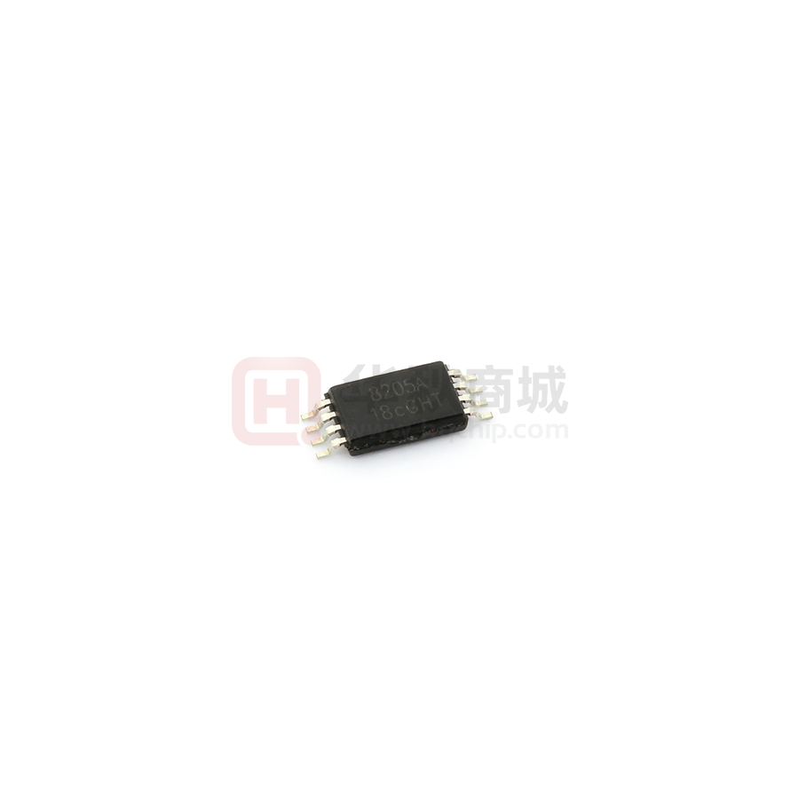
封装信息:表面安装型封装,具体封装类型为TSSOP-8。