FP6291
1MHz, 2A Step-Up Current Mode PWM Converter
Generral Description
The FP6291 is a current mode boost DC-DC converter. Its PWM circuitry with built-in 0.2Ω power
MOSFET make this regulator highly power efficient. The internal compensation network also minimizes
as much as 6 external component counts. The non-inverting input of error amplifier connects to a 0.6V
precision reference voltage and internal soft-start function can reduce the inrush current.
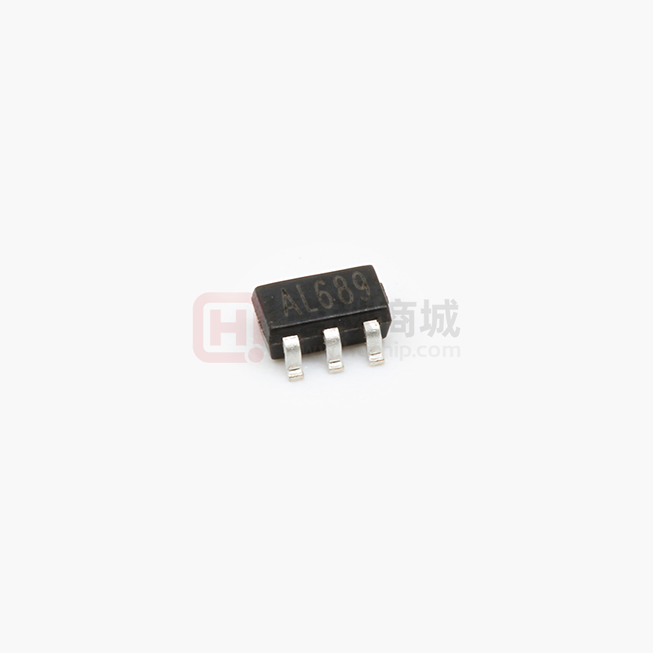
The FP6291 is available in the SOT23-6L package and provides space-saving PCB for the
application fields.
Features
� Adjustable Output up to 12V
� Internal Fixed PWM frequency: 1.0MHz
� Precision Feedback Reference Voltage: 0.6V (±2%)
� Internal 0.2Ω, 2A, 16V Power MOSFET
� Shutdown Current: 0.1µA
� Over Temperature Protection
� Adjustable Over Current Protection: 0.5A ~ 2.5A
� Package: SOT23-6L
Applications
� Chargers
� LCD Displays
� Digital Cameras
� Handheld Devices
� Portable Products
Typical Application Circuit
This datasheet contains new product information. Feeling Technology reserves the rights to modify the product specification without notice.
No liability is assumed as a result of the use of this product. No rights under any patent accompany the sales of the product.
Website: http://www.feeling-tech.com.tw
Rev. 0.66
1/10
�FP6291
Function Block Diagram
Pin Descriptions
Name
SOT23-6L
Top View
LX
1
6
OC
GND
2
5
VCC
FB
3
4
EN
No. I / O
Description
LX
1
O
Power Switch Output
GND
2
P
IC Ground
FB
3
I
Error Amplifier Inverting Input
EN
4
I
Enable Control (Active High)
VCC
5
P
IC Power Supply
OC
6
I
Adjustable Current Limit (Floating Available)
This datasheet contains new product information. Feeling Technology reserves the rights to modify the product specification without notice.
No liability is assumed as a result of the use of this product. No rights under any patent accompany the sales of the product.
Website: http://www.feeling-tech.com.tw
Rev. 0.66
2/10
�FP6291
Marking Information
SOT23-6L
Lot Number: Wafer lot number’s last two digits
For Example: 132386TB � 86
Year: Production year’s last digit
Part Number Code: Part number identification code for this product. It should be always “AL”.
This datasheet contains new product information. Feeling Technology reserves the rights to modify the product specification without notice.
No liability is assumed as a result of the use of this product. No rights under any patent accompany the sales of the product.
Website: http://www.feeling-tech.com.tw
Rev. 0.66
3/10
�FP6291
Ordering Information
Part Number
Code
Operating Temperature
Package
MOQ
Description
AL
-40°C ~ 85°C
SOT23-6L
3000EA
Tape & Reel
FP6291LR-G1
Absolute Maximum Ratings
Parameter
Symbol
Conditions
Min.
Typ.
Max.
Unit
Supply Voltage
VCC
0
6
V
LX Voltage
VLX
0
16
V
0
6
V
EN,FB Voltage
Power Dissipation
PD
SOT23-6L @TA=25°C
455
mW
Thermal Resistance (Note1)
θJA
SOT23-6L
+220
°C / W
Junction Temperature
TJ
+150
°C
Operating Temperature
TOP
-40
+85
°C
Storage Temperature
TST
-65
+150
°C
+260
°C
Lead Temperature
(soldering, 10 sec)
Note1:
θJA is measured in the natural convection at TA=25°C on a low effective thermal conductivity test
board of JEDEC 51-3 thermal measurement standard.
IR Re-flow Soldering Curve
This datasheet contains new product information. Feeling Technology reserves the rights to modify the product specification without notice.
No liability is assumed as a result of the use of this product. No rights under any patent accompany the sales of the product.
Website: http://www.feeling-tech.com.tw
Rev. 0.66
4/10
�FP6291
Recommended Operating Conditions
Parameter
Symbol
Supply Voltage
VIN
Operating Temperature Range
TA
Conditions
Ambient Temperature
Min.
Typ.
Max.
Unit
2.6
5.5
V
-40
+85
°C
DC Electrical Characteristics (VCC=3.3V, TA=25°C,unless otherwise specified)
Parameter
Symbol
Conditions
Min.
Typ.
Max.
Unit
5.5
V
System Supply Input
Input Supply Range
VCC
Under Voltage Lockout
2.6
VUVLO
UVLO Hysteresis
2.2
V
0.1
V
Quiescent Current
ICC
VFB=0.66V, No switching
0.19
mA
Average Supply Current
ICC
VFB=0.55V, Switching
2.84
mA
Shutdown Supply Current
ICC
VEN=GND
0.1
µA
FOSC
VFB=1.0V
Oscillator
Operation Frequency
Frequency Change with Voltage
0.8
△f / △V VCC=2.6V to 5.5V
Maximum Duty Cycle
TDUTY
1.0
1.2
MHZ
5
%
90
%
Reference Voltage
Reference Voltage
VREF
Line Regulation
0.588
0.6
0.612
0.05
VCC=2.6V~5.5V
V
%/V
Enable Control
Enable Voltage
VEN
Shutdown Voltage
VEN
0.96
V
0.6
V
MOSFET
On Resistance of Driver
RDS (ON) ILX=2A
Ω
0.2
Protection
OCP Current
IOCP
Adjustable OCP Current
IOCP
OTP Temperature
TOTP
With External Resistor:
10k~100k
2
2.6
A
0.5
2.5
A
+150
°C
This datasheet contains new product information. Feeling Technology reserves the rights to modify the product specification without notice.
No liability is assumed as a result of the use of this product. No rights under any patent accompany the sales of the product.
Website: http://www.feeling-tech.com.tw
Rev. 0.66
5/10
�FP6291
Typical Operating Characteristics
(VCC=3.3V, VOUT=5V, T A= 25°C, unless otherwise noted)
Current Limit vs. External Resistance (Roc)
Efficiency vs. Output Current
100
3.5
95
3
2.5
Current Limit (A)
Efficiency (%)
90
85
80
2
1.5
1
75
0.5
70
0
0
0.1
0.2
0.3
0.4
0.5
0.6
0.7
0.8
0.9
1
10
20
30
40
60
70
80
90
100
Operation Frequency vs. Temperature
Operation Frequency vs. Input Voltage
1.1
1.16
1.14
Operation Freqency (MHz)
Operation Frequency (MHz)
50
External Resistance (kΩ)
Output Current (A)
1.12
1.1
1.08
1.06
1.04
1.08
1.06
1.04
1.02
1.02
VIN =5V, VOUT =9V
1
2
3
4
5
6
-40
-20
0
Input Voltage (V)
20
40
60
80
100
Temperature (°C)
Reference Voltage vs. Input Voltage
Reference Voltage vs. Output Current
0.607
0.605
Feedback Voltage (V)
Feedback Voltage (V)
0.606
0.605
0.604
0.603
0.602
0.601
0.604
0.603
0.602
0.601
0.6
0.6
2
3
4
5
6
0
0.1
0.2
0.3
Input Voltage (V)
Quiescent Current vs. Input Voltage
0.5
0.6
0.7
0.8
0.9
1
Average Supply Current vs. Input Voltage
270
4.5
Average Supply Current (mA)
Quiescent Current (uA)
0.4
Output Current (A)
240
210
180
150
120
4
3.5
3
2.5
2
1.5
1
0.5
2
3
4
5
6
2
Input Voltage (V)
3
4
5
6
Input Voltage (V)
This datasheet contains new product information. Feeling Technology reserves the rights to modify the product specification without notice.
No liability is assumed as a result of the use of this product. No rights under any patent accompany the sales of the product.
Website: http://www.feeling-tech.com.tw
Rev. 0.66
6/10
�FP6291
Function Description
Operation
The FP6291 is a current mode boost converter. The constant switching frequency is 1MHz and
operates with pulse width modulation (PWM). Build-in 16V / 2A MOSFET provides a high output
voltage. The control loop architecture is peak current mode control; therefore slope compensation
circuit is added to the current signal to allow stable operation for duty cycles larger than 50%.
Soft Start Function
Soft start circuitry is integrated into FP6291 to avoid inrush current during power on. After the IC
is enabled, the output of error amplifier is clamped by the internal soft-start function, which causes
PWM pulse width increasing slowly and thus reducing input surge current.
Current Limit Program
A resistor between OC and GND pin programs peak switch current. The resistor value should be
between 10k and 100k. The current limit will be set from 2.5A to 0.5A. Keep traces at this pin as short
as possible. Do not put capacitance at this pin. To set the over current trip point according to the
following equation:
IOCP =
48000
R3
Over Temperature Protection (OTP)
FP6291 will turn off the power MOSFET automatically when the internal junction temperature is
over 150°C. The power MOSFET wake up when the junction temperature drops 30°C under the OTP
threshold temperature.
Output Disconnect
When power on and the EN pin will be pulled high. The FP6291 start up and operates. The
external PMOS is turned on and current through it for output loading. While output loading is increase,
output voltage is drop. When the FB pin voltage is under 0.3V, the EN pin sinks 20µA current, the
external PMOS will be turn off. The output short condition will be disconnected.
This datasheet contains new product information. Feeling Technology reserves the rights to modify the product specification without notice.
No liability is assumed as a result of the use of this product. No rights under any patent accompany the sales of the product.
Website: http://www.feeling-tech.com.tw
Rev. 0.66
7/10
�FP6291
Application Information
Inductor Selection
Inductance value is decided based on different condition. 3.3uH to 4.7µH inductor value is
recommended for general application circuit. There are three important inductor specifications, DC
resistance, saturation current and core loss. Low DC resistance has better power efficiency.
Also, it
avoid inductor saturation which will cause circuit system unstable and lower core loss at 1 MHz.
Capacitor Selection
The output capacitor is required to maintain the DC voltage. Low ESR capacitors are preferred to
reduce the output voltage ripple. Ceramic capacitor of X5R and X7R are recommended, which have
low equivalent series resistance (ESR) and wider operation temperature range.
Diode Selection
Schottky diodes with fast recovery times and low forward voltages are recommended. Ensure the
diode average and peak current rating exceed the average output current and peak inductor current. In
addition, the diode’s reverse breakdown voltage must exceed the output voltage.
Output Voltage Programming
The output voltage is set by a resistive voltage divider from the output voltage to FB. The output
voltage is:
R1
VOUT = 0.6 V 1 +
R2
Layout Considerations
1. The power traces, consisting of the GND trace, the LX trace and the VCC trace should be kept
short, direct and wide.
2. LX、L and D switching node, wide and short trace to reduce EMI.
3. Place CIN near VCC pin as closely as possible to maintain input voltage steady and filter out the
pulsing input current.
4. The resistive divider R1and R2 must be connected to FB pin directly as closely as possible.
5. FB is a sensitive node. Please keep it away from switching node, LX.
6. The GND of the IC, CIN and COUT should be connected close together directly to a ground
plane.
This datasheet contains new product information. Feeling Technology reserves the rights to modify the product specification without notice.
No liability is assumed as a result of the use of this product. No rights under any patent accompany the sales of the product.
Website: http://www.feeling-tech.com.tw
Rev. 0.66
8/10
�FP6291
Typical Application
General Boost Converter
SCP Detect and Load Disconnect
This datasheet contains new product information. Feeling Technology reserves the rights to modify the product specification without notice.
No liability is assumed as a result of the use of this product. No rights under any patent accompany the sales of the product.
Website: http://www.feeling-tech.com.tw
Rev. 0.66
9/10
�FP6291
Package Outline
SOT23-6L
Unit: mm
Symbols
Min. (mm)
Max. (mm)
A
1.050
1.450
A1
0.050
0.150
A2
0.900
1.300
b
0.300
0.500
c
0.080
0.220
D
2.900 BSC
E
2.800 BSC
E1
1.600 BSC
e
0.950 BSC
e1
1.900 BSC
L
0.300
0.600
L1
0.600 REF
L2
0.250 BSC
θ°
θ1°
θ2°
0°
8°
3°
7°
6°
15°
Note:
1. Package dimensions are in compliance with JEDEC outline: MO-178 AB.
2. Dimension “D” does not include molding flash, protrusions or gate burrs.
3. Dimension “E1” does not include inter-lead flash or protrusions.
This datasheet contains new product information. Feeling Technology reserves the rights to modify the product specification without notice.
No liability is assumed as a result of the use of this product. No rights under any patent accompany the sales of the product.
Website: http://www.feeling-tech.com.tw
Rev. 0.66
10/10
�
很抱歉,暂时无法提供与“FP6291LR-G1”相匹配的价格&库存,您可以联系我们找货
免费人工找货- 国内价格
- 5+0.66400
- 20+0.60400
- 100+0.54400
- 500+0.48400
- 1000+0.45600
- 2000+0.43600