GBLC03CI thru GBLC24CI
TVS Array
The GBLCxxCI Series is ultra low capacitance transient voltage suppressor arrays, designed to protect applications
such as portable electronics and SMART phones. This series is available in both unidirectional and bidirectional
configurations and is rated at 350 Watts for an 8/20μs waveform.
The GBLCxxCI Series meets IEC 61000-4-2 (ESD) and IEC 61000-4-4 (EFT) requirements. At higher operating
frequencies or faster edge rates, insertion loss and signal integrity are a major concern. This series offers an ultra low
capacitance and low leakage current in a miniature SOD-323 package.
Features
350 Watts Peak Pulse Power per Line (8 x 20 us Waveform)
Replacement for MLV (0805)
Protects One Power or I/O Port
Low Clamping Voltage
Available in Multiple Voltages Ranging From 3V to 24V
Ultra Low Capacitance: 0.8pF (Typical)
Response Time is < 1 ns
Meets MSL 1 Requirements
Solid-state silicon avalanche technology
ROHS compliant
WeiPan technology
Main applications
Hand−Held Portable Applications
Networking and Telecom(Ethernet 10/100/1000 Base T)
USB Interface
Automotive Electronics
Serial and Parallel Ports
Notebooks, Desktops, Servers
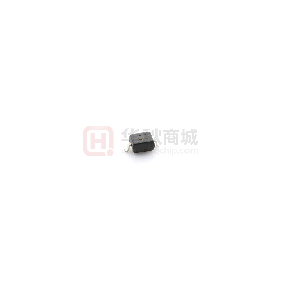
SOD323
Protection solution to meet
IEC61000-4-2 (ESD) ±15kV (air), ±8kV (contact)
IEC61000-4-4 (EFT) 40A (5/50ns)
1/4
�GBLC03CI thru GBLC24CI
TVS Array
Maximum ratings (Tamb=25℃ Unless Otherwise Specified)
Parameter
Peak Pulse Power (tp=8/20μs waveform)
ESD Rating per IEC61000-4-2:
Symbol
Value
Unit
PPPP
350
Watts
Contact
8
Air
15
KV
Lead Soldering Temperature
TL
260 (10 sec.)
℃
Operating Temperature Range
TJ
-55 ~ 150
℃
TSTG
-55 ~ 150
℃
TL
260
℃
Storage Temperature Range
Lead Solder Temperature − Maximum (10 Second Duration)
Maximum ratings are those values beyond which device damage can occur. Maximum ratings applied to the device are individual stres s limit values (not
normal operating conditions) and are not valid simultaneously. If these limits are exceeded, device functional operation is not implied, damage may occur
and reliability may be affected.
*Other voltages may be available upon request.
1. Non-repetitive current pulse, per Figure 1.
Electrical characteristics ( Tamb=25℃ Unless Otherwise Specified)
VRWM
VBR @ 1 mA
VC
(Volts)
@1A
Max IPP
IR @ VRWM
Device
Capacitance
@ VR = 0 V, 1
PPK
MHz (pF)
(V)
(uA)
Min
(V)
(A)
Typ
(W)
GBLC03CI
3
5
4.00
7.50
22
0.8
350
GBLC05CI
5
2
6.00
9.80
20
0.8
350
GBLC08CI
8
1
8.50
13.6
13
0.8
350
GBLC12CI
12
1
13.3
19.0
10
350
GBLC15CI
15
1
16.7
24.0
8.0
0.8
0.8
GBLC24CI
24
1
26.7
43.0
6.0
0.8
350
350
Junction capacitance is measured in VR=0V,F=1MHz
I
Symbol
VRWM
IPP
Parameter
Working Peak Reverse Voltage
VBR
Breakdown Voltage @ IT
VC
Clamping Voltage @ IPP
IT
Test Current
IRM
Leakage current at VRWM
IPP
Peak pulse current
CO
Off-state Capacitance
CJ
Junction Capacitance
VC
VBR VRWM
IT
IR
IR
IT
IPP
2/4
VRWM
VBR
VC
V
�GBLC03CI thru GBLC24CI
TVS Array
Typical electrical characterist applications
10
Waveform
Parameters:
tr=8us
td=20us
Peak Pulse Power-P PK(KW)
PP
110
100
90
80
70
60
50
40
30
20
10
0
td=IPP/2
0
5
10
15
20
25
30
% of Rated Power or Ipp
110
100
90
80
70
60
50
40
30
20
10
0
50
75
0.01
0.1
1
10
100
1000
Non-Repetitive Peak Pulse Power vs. Pulse Time
Pulse Waveform
25
0.1
Pulse Duration-tp(us)
Time (us)
0
1
100
125
150
Ambient Temperature-TA
Power Derating Curve
3/4
�GBLC03CI thru GBLC24CI
TVS Array
Package Information
Mechanical Data
Case: SOD-323
Case Material: Molded Plastic. UL Flammability
K
A
Millimeters
Dim
D
2
1
A
B
E
J
Min
Max
Min
Max
1.60
1.80
0.063
0.071
B
1.2
1.40
0.047
0.055
C
0.80
0.90
0.031
0.035
D
0.25
0.35
0.010
0.014
0.15REF
E
C
Inches
0.006REF
H
0
0.10
0
0.004
J
0.08
0.15
0.003
0.006
K
2.50
2.70
0.098
0.106
H
SOD-123
Recommended Pad outline
0.7
2.15
0.7
SOD-323 Reel Dim
E
P0
K
P2
D
W
F
D1
A0
T
B0
B1
K0
P1
Package
Pocket Size
Tape
B0×A0×K0(mm)
Width
Chip Size
Reel Diameter
Quantity Per Reel
P0
P1
4mm
4mm
SOD-323
2.60×1.40×1.05
3.30×1.50×1.25
8mm
178mm(7")
3000
D0
D1
E
F
K
T
W
1.5mm
0.5mm
1.75mm
3.5mm
0.95mm
0.2mm
8mm
4/4
�
很抱歉,暂时无法提供与“GBLC03CI”相匹配的价格&库存,您可以联系我们找货
免费人工找货- 国内价格
- 5+0.23300
- 50+0.19210
- 150+0.16330
- 500+0.14780
- 3000+0.13500