CHIP DIODE
Switching Diode
CD4148WTP
1:6
Switching Diode
CD4148WTP
FEATURES
Silicon epitaxial planar diode
SMD chip pattern, available in various dimension included 1206 & 0805
Leadfree and RoHS compliance components
For small signal switching and operating ambient temperature less than 55oC and voltage withstand
less than 60V; not suitable for AC switching input as rectified circuit and high reverse voltage
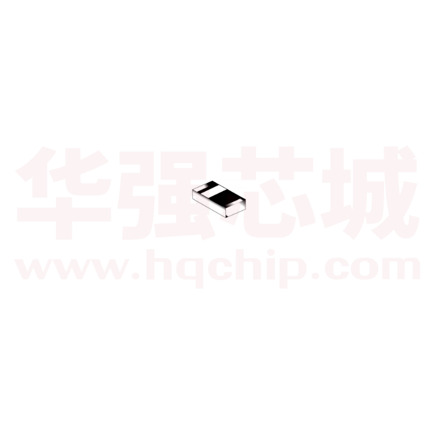
location
MECHANICAL CHARACTERISTICS
Size: 0603
Weight: approx. 4mg
Marking: Cathode terminal
DIMENSIONS
Dimension/mm
0603
L
W
T
C
1.55±0.1
0.80±0.1
0.65±0.1
0.35±0.1
THERMAL CHARACTERISTICS1)
Parameter at Tamb=25oC1)
Symbol
Forward Power Dissipation
Power derating above 25oC
Ptot
Junction Temperature
Thermal Resistance Junction to Ambient air
Operating& Storage Temperature range
Tj
RθJA
Tstg
Value
Unit
200
mW
1.6
mW/ oC
150
375
-55 to 150
o
C
C/W
o
C
o
1) Valid provided that electrodes are kept at ambient temperature.
www.lizgroup.com
Ref No: CD4148WTP
V3.2
NOV 25, 2009
�CHIP DIODE
Switching Diode
CD4148WTP
2:6
MAXIMUM RATING1)
Parameter at Tamb=25oC1)
Symbol
Value
Unit
VRRM
75
V
IF(AV)
100
mA
IFRM
200
mA
400
mA
800
mA
Value
Unit
1.0 MAX
1.25 MAX
0.025 MAX
5 MAX
4 MAX
4 MAX
V
V
uA
uA
pF
ns
Repetitive Peak Reverse Voltage
Average rectified current sin half wave
rectification with resistive load
Repetitive Peak Forward Current at Tamb=25°C
Non-Repetitive Surge Forward Current
at t95% area tin covered
Resistance to Soldering Heat
Sn bath at 260±5oC for 10±2s
VF,VR & IR within spec;
no mechanical damage
Humidity Steady State
At 85oC 85%RH for 168hrs
VF,VR & IR within spec
Continue Forward Operating Life
At 25oC IF =1.1IF for 1000hrs
VF,VR & IR within spec
o
o
Thermal Shock
-55 ±5 C/5min to 150±5 C/5min
for 10cycles
VF,VR & IR within spec
Bending Strength
Bending up to 2mm for 1cycle
VF,VR & IR within spec;
no mechanical damage
www.lizgroup.com
Ref No: CD4148WTP
V3.2
NOV 25, 2009
�CHIP DIODE
Switching Diode
CD4148WTP
4:6
APPLICATIONS
Function: suit for small signal switching application
Typical Application circuit:
Typical Product field: General application except high reverse voltage location
Soldering Condition:
Soldering Condition & Caution
■ Recommended Soldering Condition
(Refer to IPC/JEDEC J-STD-020D 4-1&5.2)
Recommended Profile Condition
Ramp-up rate (from pre-heat stage)
Pre-heat Temperature & Time
Soldering Temperature & Time
Peak Temperature
Time within 5oC of peak temperature
Ramp-down rate
Time 25oC to peak temperature
Sn-Pb Soldering
o
很抱歉,暂时无法提供与“CD4148WTP”相匹配的价格&库存,您可以联系我们找货
免费人工找货- 国内价格
- 50+0.12074
- 500+0.10867
- 5000+0.10062
- 10000+0.09660
- 30000+0.09257
- 50000+0.09016
- 国内价格
- 20+0.29840
- 100+0.17800
- 500+0.12470
- 5000+0.08900
- 10000+0.08450
- 50000+0.07830


 工商网监
湘ICP备2023018690号
工商网监
湘ICP备2023018690号