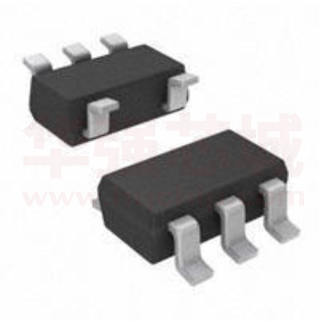
HX6219
300mA,Ultra-low noise, Small Package
Ultra-Fast CMOS LDO Regulator
General Description
Features
The 6219 is designed for portable RF and wireless
Ultra-Low-Noise for RF Application
applications with demanding performance and space
2.5V- 5.5V Input Voltage Range
requirements. The 6219 performance is optimized for
Low Dropout : 220mV @ 300mA
battery-powered systems to deliver ultra low noise and
1.8V, 2.8V,3.0V and 3.3V Fixed
low quiescent current. The 6219 also works with low-ESR
300mA Output Current, 550mA Peak Current
ceramic capacitors, reducing the amount of board space
High PSSR:-76dB at 1KHz
necessary for power applications, critical in hand-held
< 0.01uA Standby Current When Shutdown
wireless devices. The 6219 consumes less than 0.01µA
Available in SOT23-5 and TSOT23-5 Package
in shutdown mode and has fast turn-on time less than
TTL-Logic-Controlled Shutdown Input
50µs. The other features include ultra low dropout voltage,
Ultra-Fast Response in Line/Load transient
high output accuracy, current limiting protection, and high
Current Limiting and Thermal Shutdown Protection
Quick start-up (typically 50uS)
ripple rejection ratio.
It is available in the 5-lead of
SOT23-5 and TSOT23-5 packages.
Typical Application Circuit
Ordering Information
HX6219 □ □
□ □
□
F: Pb-Free
Package Type
B3: SOT23-3
B5: SOT23-5
J5: TSOT23-5
Output Voltage Type
18: 1.8V
Applications
25: 2.5V
Portable Media Players/MP3 players
28: 2.8V
Cellular and Smart mobile phone
30: 3.0V
LCD
33: 3.3V
DSC Sensor
Wireless Card
Page 1 of 8
�HX6219
Pin Configurations
Top View
VIN
1
GND
2
EN
3
Top View
VOUT
5
VIN
4
2
VOUT
1
GND
3
NC
TSOT23-5/SOT-23-5
SOT-23-3
Functional Pin Description
SOT23-5
SOT23-3
Pin Name
Pin Function
1
3
VIN
Power Input Voltage.
2
1
GND
Ground.
3
-
EN
Chip Enable (Active High).
4
-
NC
No Connection.
5
2
VOUT
Output Voltage.
Page 2 of 8
�HX6219
Function Block Diagram
Absolute Maximum Ratings
Supply Input Voltage ------------------------------------------------------------------------------------------------------------------------------------- 6.5V
Other Pin Voltage ----------------------------------------------------------------------------------------------------------------------- -0.3V to VIN+0.3V
Power Dissipation, PD @ TA = 25°C
T/SOT23-5 ---------------------------------------------------------------------------------------------------------------------------------------------- 500mW
SOT23-3 ------------------------------------------------------------------------------------------------------------------------------------------------ 500mW
Package Thermal Resistance
Thermal Resistance(SOT23-5/SOT23) (JA) ------------------------------------------------------------------------------------------------- 195℃/W
Thermal Resistance(SOT23-5/SOT23) (JC) --------------------------------------------------------------------------------------------------- 60℃/W
Maximum Junction Temperature -------------------------------------------------------------------------------------------------------------------- 150℃
Maximum Soldering Temperature (at leads, 10 sec) ------------------------------------------------------------------------------------------ 260℃
Storage Temperature Range ----------------------------------------------------------------------------------------------------------- −65℃ to 150℃
ESD Susceptibility
HBM (Human Body Mode) ----------------------------------------------------------------------------------------------------------------------------- 2KV
MM(Machine-Mode) ------------------------------------------------------------------------------------------------------------------------------------- 200V
Page 3 of 8
�HX6219
Recommended Operating Conditions
Supply Input Voltage -------------------------------------------------------------------------------------------------------------------------- 2.5V to 5.5V
EN Input Voltage ----------------------------------------------------------------------------------------------------------------------------- 0V toVin+0.3V
Operation Junction Temperature Range --------------------------------------------------------------------------------------------- −40°C to 125°C
Operation Ambient Temperature Range ---------------------------------------------------------------------------------------------- −40°C to 85°C
Electrical Characteristics
(VIN = VOUT + 1V, CIN = COUT = 1µF, TA = 25° C, unless otherwise specified)
Parameter
Symbol
Test Conditions
Min
Typ.
Max
Units
Output Voltage Accuracy
ΔVOUT
IOUT =1mA
−2
--
+2
%
Output Loading Current
ILO AD
VEN =VIN , V IN >2.5V
Current Limit
IL IM
RLOAD = 1Ω
Quiescent Current
IQ
VEN ≥1.2V, IOUT =0mA
100
130
Dropout Voltage
VDROP
IOUT =200mA, V OUT >2.8V
130
200
IOUT =300mA, V OUT >2.8V
220
300
Line Regulation
ΔVLINE
Load Regulation
ΔILOAD
1mA 25mΩ on the
Where TJ(MAX) is the maximum operation junction
6219 output ensures stability. The 6219 still works well
temperature 125°C, TA is the ambient temperature and
with output capacitor of other types due to the wide stable
the θJA is the junction to ambient thermal resistance. For
ESR range. Output capacitor of larger capacitance can
recommended operating conditions specification of 6219,
reduce noise and improve load transient response,
where TJ(MAX) is the maximum junction temperature of
stability, and PSRR. The output capacitor should be
the die (125°C) and TA is the maximum ambient
located not more than 0.5 inch from the VOUT pin of the
temperature. The junction to ambient thermal resistance
6219 and returned to a clean analog ground.
(θJA is layout dependent) for SOT23-5 package is
Start-up Function Enable Function
195°C/W.
PD(MAX) = ( 125°C − 25°C ) / 195 = 500mW
The 6219 features an LDO regulator enable/disable
The maximum power dissipation depends on operating
function. To assure the LDO regulator will switch on, the
ambient temperature for fixed TJ(MAX) and thermal
EN turn on control level must be greater than 1.4 volts.
resistance θJA.
The LDO regulator will go into the shutdown mode when
the voltage on the EN pin falls below 0.4 volts. For to
protecting the system, the 6219 have a quick-discharge
function. If the enable function is not needed in a specific
application, it may be tied to VIN to keep the LDO
regulator in a continuously on state.
Page 5 of 8
�HX6219
Packaging Information
SOT23-5
Page 6 of 8
�HX6219
Page 7 of 8
�HX6219
SOT23-3
Page 8 of 8
�
很抱歉,暂时无法提供与“HX6219B332MR”相匹配的价格&库存,您可以联系我们找货
免费人工找货- 国内价格
- 50+0.12000
- 500+0.10800
- 5000+0.10000
- 10000+0.09600
- 30000+0.09200
- 50000+0.08960
