HX6306
300mA Low Power LDO
Features
Low power consumption
Low Quiescent Current: 3uA at 6V
Low voltage drop
Output voltage accuracy: tolerance ±2%
Low temperature coefficient
Applications
Battery-powered equipment
Portable AV systems
Reference voltage sources
Mobile phones
Cameras,video cameras
Portable games
General Description
HX6306 series are a highly precise, lower
compatible with low ESR ceramic capacitors. The
consumption,
voltage
current limiter’s foldback circuit operates as a
regulators manufactured using CMOS and laser
short circuit protection as well as the output
trimming technologies. The series provides large
current limiter for the output pin. Output voltages
currents
are internally by laser trimming technologies. It is
with
3
a
terminal,positive
significantly
small
dropout
voltage .
selectable in 0.1V increments within a range of
The HX6306 consists of a current limiter circuit, a
1.2V to 5.0V.
driver transistor, a precision reference voltage
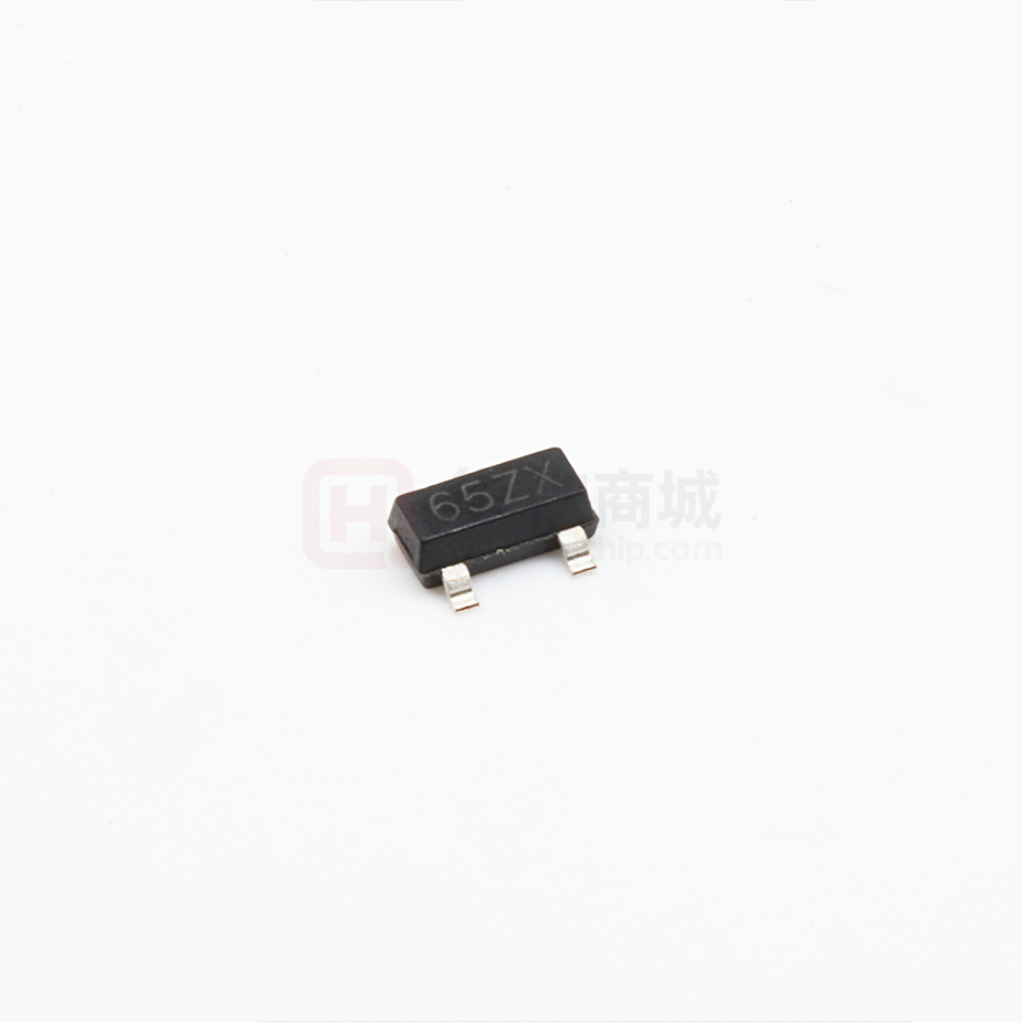
SOT-23 、SOT23-3and SOT-89 packages.
and an error correction circuit.
HX6306 series are available in
The series is
Typical Application
Order Information
HX6306- ①②③④
Designator
①②
③
④
Symbol
Integer
N
M
P
P1
R
G
Description
Output Voltage(2.1~5.0V)
Package:SOT23
Package:SOT23-3
Package:SOT89A
Package:SOT89B
RoHS / Pb Free
Halogen Free
Note:”①②” stands for output voltages. Other voltages can be specially customized
1
�HX6306
300mA Low Power LDO
Block Diagram
Pin Assignment
2
�HX6306
300mA Low Power LDO
Marking Rule
① represents product number
MARK
6
PRODUCT SERIES
HX6306****
② represents 3 pins regulator
MARK
VOLTAGE=0.1~3.0V VOLTAGE=3.1V~6.0V
5
6
③ represents output voltage
MARK
VOLTAGE(V)
0
3.1
1
3.2
2
3.3
3
3.4
4
3.5
5
3.6
6
3.7
7
3.8
8
3.9
9
4.0
A
4.1
B
1.2
4.2
C
1.3
4.3
D
1.4
4.4
E
1.5
4.5
MARK
F
H
K
L
M
N
P
R
S
T
U
V
X
Y
Z
-
④ X
3
1.6
1.7
1.8
1.9
2.0
2.1
2.2
2.3
2.4
2.5
2.6
2.7
2.8
2.9
3.0
PRODUCT
SERIES
HX6306
VOLTAGE(V)
4.6
4.7
4.8
4.9
5.0
-
-
�HX6306
300mA Low Power LDO
Absolute Maximum Ratings
Parameter
Input Voltage
Output Current
Output Voltage
SOT-23
SOT-89
Power Dissipation
USP-6B
TO-92
Operating Temperature Range
Storage Temperature Range
Symbol
VIN
IOUT
VOUT
Pd
Topr
Tstg
Ratings
10
300*
VSS-0.3~VIN+0.3
0.20
0.50
0.10
0.30
-40~+85
-55~+125
Units
V
mA
V
W
W
W
W
℃
℃
*IOUT=Pd/(VIN-VOUT)
Electrical Characteristics
(Ta=25℃)
HX6306 for any output voltage
Parameter
Symbol
Output Voltage
Vout
Output Current*1
Iout
Low dropout*2
Vdrop
Line Regulation
△Vout1/(Vin·Vout)
Load Regulation
△Vout /ΔIout
Output voltage
Temperature
△Vout/(Ta·Vout)
Coefficiency
Conditions
Vin=Vout+1V
1.0mA≤Iout≤30mA
Vin-Vout=1V
Min.
Typ.
Max.
Unit
Vout×0.98
--
Vout×1.02
V
--
300
--
mA
Refer to the next table
1.6V≤Vin≤8V
Iout=40mA
Vin= Vout+1V
1.0mA≤Iout≤80mA
Iout=30mA
0℃≤Ta≤70℃
--
0.05
0.2
%/V
--
12
30
mV
--
±100
--
Ppm/℃
Supply Current
Iss
--
--
3
5
uA
Input Voltage
Vin
--
--
8
10
V
PSRR
PSRR
--
50
--
dB
Output Noise
EN
--
30
--
uVrms
F=1KHz
Vin=Vout+1V
BW=10Hz~100KHz
4
�HX6306
300mA Low Power LDO
Electrical Characteristics by Output Voltage:
Output Voltage Vout(V)
Dropout Voltage Vdif(V)
Conditions
Vout≤1.5V
1.8 ≤ Vout ≤ 2
Iout=100 mA
2.8 ≤ Vout ≤ 5.0
Typ.
Max.
0.35
0.57
0.28
0.42
0.19
0.35
Typical Performance Characteristics
(1) Output Voltage vs Input voltage and Output Voltage vs.Output Current and
Input Transient Response
HX6306
HX6306
HX6306
(2) Output Voltage vs. Ambient Temperature
HX6306
5
�HX6306
300mA Low Power LDO
Package Information
3-pin SOT23 Outline Dimensions
6
�HX6306
300mA Low Power LDO
3-pin SOT23-3 Outline Dimensions
7
�HX6306
300mA Low Power LDO
3-pin SOT89 Outline Dimensions
8
�
很抱歉,暂时无法提供与“HX6306P302MR”相匹配的价格&库存,您可以联系我们找货
免费人工找货