Techcode®
DATASHEET
High-Performance PWM Controller
TD1730
General Description
Features
The TD1730 is a single‐phase, constant‐on‐time,
synchronous PWM controller, which drives N‐channel
MOSFETs. The TD1730 steps down high voltage to
generate low‐voltage chipset or RAM supplies in notebook
computers.
The TD1730 provides excellent transient response and
accurate DC voltage output in either PFM or PWM Mode. In
Pulse Frequency Mode (PFM), the TD1730 provides very high
efficiency over light to heavy loads with loading‐ modulated
switching frequencies. In PWM Mode, the converter works
nearly at constant frequency for low‐noise requirements.
The TD1730 is equipped with accurate positive current‐ limit,
output under‐voltage, and output over‐voltage
protections, perfect for NB applications. The Power‐On‐
Reset function monitors the voltage on VCC to prevent
wrong operation during power‐on. The TD1730 has a 1ms
digital soft‐start and built‐in an integrated output
discharge method for soft‐stop. An internal integrated
soft‐start ramps up the output voltage with programmable
slew rate to reduce the start‐up current. A soft‐stop function
actively discharges the output capacitors with controlled
reverse inductor current.
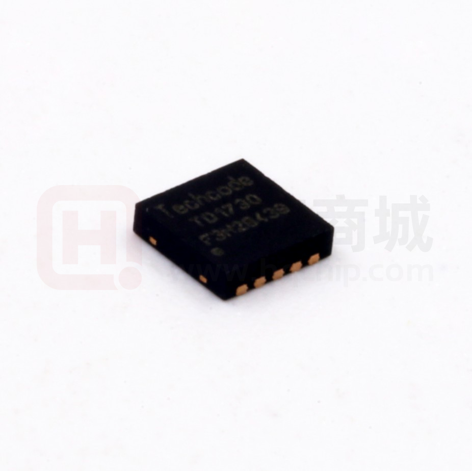
The TD1730 is available in 10pin TDFN 3x3 package.
z
z
z
z
z
z
z
z
z
z
z
z
z
z
z
z
z
z
z
z
z
Adjustable Output Voltage from +0.7V to +5.5V
0.7V Reference Voltage
±1% Accuracy Over‐Temperature
Operates from an Input Battery Voltage Range of +1.8V
to +32V
Power‐On‐Reset Monitoring on VCC Pin
Excellent Line and Load Transient Responses
PFM Mode for Increased Light Load Efficiency
Selectable PWM Frequency from 4 Preset Values
Integrated MOSFET Drivers
Integrated Bootstrap Forward P‐CH MOSFET
Adjustable Integrated Soft‐Start and Soft‐Stop
Selectable Forced PWM or Automatic PFM/PWM Mode
Power Good Monitoring
70% Under‐Voltage Protection
125% Over‐Voltage Protection
Adjustable Current‐Limit Protection
Using Sense Low‐Side MOSFET’s RDS(ON)
Over‐Temperature Protection
Auto Rework from Protection Mode
TDFN‐10 3x3 Package
Lead Free and Green Devices Available (RoHS Compliant)
Applications
z
z
z
z
Notebook
Table PC
Hand‐Held Portable
AIO PC
z
LCD Monitor / TV
z
Battery Charger
z
ADSL Modem
z
Telecom / Networking Equipment
December, 20, 2011 Techcode Semiconductor Limited www.techcodesemi.com
1
�Techcode®
DATASHEET
High-Performance PWM Controller
TD1730
Pin Assignments
GND and Thermal Pad (connected to GND plane for better heat dissipation)
PIN
FUNCTION
NO.
TDFN3x3
TDFN2x2
1
1
2
2
3
3
4
4
5
‐
6
6
7
7
8
8
9
9
10
10
Exposed
Pad
NAME
5
Power Good Output. POK is an open drain output used to indicate the status of the output voltage.
Connect the POK in to +5V through a pull‐high resistor.
Current‐Limit Threshold Setting Pin. There is an internal source current 10 uA through a resistor from
OCSET OCSET pin to GND. This pin is used to monitor the voltage drop across the Drain and Source of the
low‐side MOSFET for current‐limit.
Enable Pin of The PWM Controller. When the EN is above enable logic level, the Device is workable.
EN When the EN is below shutdown logic level, the device is in shutdown and only low leakage current is
taken from VCC and VIN.
Output Voltage Feedback Pin. This pin is connected to the resistive divider that set the desired output
FB voltage. The POK, UVP, and OVP circuits detect this signal to report output voltage status.
This Pin is Allowed to Adjust The Switching Frequency. Connect a resistor RRF to set switching
frequency as show in Table1. The pin also controls forced PWM mode or PFM/PWM auto skip mode
RF selection. When RF pin is pulled down to GND, the device is in automatic PFM/PWM Mode. When RF pin
is pulled high to POK, the device is in force PWM mode.
POK
Output of The Low‐side MOSFET Driver. Connect this pin to Gate of the low‐side
LGATE MOSFET. Swings from GND to VCC.
Supply Voltage Input Pin for Control Circuitry. Connect +5V from the VCC pin to the GND pin.
VCC Decoupling at least 1u F of a MLCC capacitor from the VCC pin to the GND pin.
Junction Point of The High‐side MOSFET Source, Output Filter Inductor and The
PHASE Low‐side MOSFET Drain. Connect this pin to the Source of the high‐side MOSFET. PHASE serves as the
lower supply rail for the UGATE high‐side gate driver.
UGATE Output of The High‐side MOSFET Driver. Connect this pin to Gate of the high‐side MOSFET.
Supply Input for The UGATE Gate Driver and An Internal Level‐shift Circuit. Connect to an external
BOOT capacitor to create a boosted voltage suitable to drive a logic‐level N‐channel
MOSFET.
GND Signal Ground for The IC
December, 20, 2011 Techcode Semiconductor Limited www.techcodesemi.com
2
�
Techcode®
DATASHEET
High-Performance PWM Controller
TD1730
Ordering Information
TD1730 □
□
Circuit Type Packing:
Blank:Tube
R:Type and Reel
Package
Q:TDFN
Functional Block Diagram
Functional Block Diagram of TD1730
December, 20, 2011 Techcode Semiconductor Limited www.techcodesemi.com
3
�Techcode®
DATASHEET
High-Performance PWM Controller
TD1730
Absolute Maximum Ratings
Symbol
VCC
VBOOT‐GND
VBOOT
Parameter
VCC Supply Voltage (VCC to GND)
BOOT Supply Voltage (BOOT to GND)
BOOT Supply Voltage (BOOT to PHASE)
All Other Pins (POK, OCSET, EN, FB, and RF to GND)
UGATE Voltage (UGATE to PHASE) Pulse Width 400ns
LGATE Voltage (LGATE to GND)
PHASE Voltage (PHASE to GND)
VPHASE
TJ
TSTG
TSDR
Rating
‐0.3 ~ 7
‐0.3 ~ 35
‐0.3 ~ 7
‐0.3 ~ VCC+0.3
‐5 ~ VBOOT+0.3
‐0.3 ~ VBOOT+0.3
Unit
V
V
V
V
V
Pulse Width 400ns
‐5 ~ VCC+0.3
‐0.3 ~ VCC+0.3
V
Pulse Width 400ns
‐5 ~ 35
‐1 ~ 32
V
Maximum Junction Temperature
Storage Temperature
Maximum Soldering Temperature, 10 Seconds
150
‐65 ~ 150
260
C
C
o
C
o
o
Note: Stresses beyond those listed under "absolute maximum ratings" may cause permanent damage to the device. These are stress ratings only and
functional operation of the device at these or any other conditions beyond those indicated under "recommended operating conditions" is not implied.
Exposure to absolute maximum rating conditions for extended periods may affect device reliability
Recommended Operating Conditions
Symbol
VIN
VCC
VOUT
IOUT
TA
TJ
Parameter
Converter Input Voltage
VCC Supply Voltage
Converter Output Voltage
Converter Output Current
Ambient Temperature
Junction Temperature
Range
1.8 ~32
4.5 ~ 5.5
0.7 ~ 5.5
~ 25
‐40 ~ 85
‐40 ~ 125
Unit
V
V
V
A
o
C
o
C
Note: Refer to the typical application circuit.
Thermal Characteristics
Symbol
θJA
Parameter
Thermal Resistance‐Junction to Ambient 3mmx3mm TDFN‐10
Typical Value
55
Unit
°C/W
Note: θJA is measured with the component mounted on a high effective the thermal conductivity test board in free air. The exposed pad of package is
soldered directly on the PCB.
December, 20, 2011 Techcode Semiconductor Limited www.techcodesemi.com
4
�Techcode®
DATASHEET
High-Performance PWM Controller
Electrical Characteristics
TD1730
Refer to the typical application circuit. These specifications apply over VVCC = 12V, TA = ‐40°C to 85°C, unless otherwise noted. Typical values are at TA = 25°C.
Symbol
Parameter
Test Conditions
TD1730
Unit
Min.
Typ.
Max.
VOUT AND VFB VOLTAGE
VOUT
Output Voltage
VREF
Reference Voltage
Adjustable output range
0.7
-
Regulation Accuracy
TA = 25 oC
-0.5
TA = 0 oC ~ 85 oC
-0.8
-1.0
o
o
TA = -40 C ~ 85 C
5.5
V
0.7
IFB
FB Input Bias Current
FB = 0.7V
-
0.02
TDIS
VOUT Discharge Time
EN low to FB = 0V
-
12
-
V
-
+0.5
%
-
+0.8
%
-
+1.0
%
0.1
uA
-
ms
SUPPLY CURRENT
IVCC
IVCC
SHDN
VCC Input Bias Current
VCC Shutdown Current
VCC Current, PWM, EN = 5V, VFB = 0.735V, PHASE =
-
250
0 5V
EN = GND, VCC = 5V
-
0
520 uA
1
uA
SWITCHING FREQUENCY AND SUTY AND INTERNAL SOFT-START
RRF = 470k
RRF = 200k
FSW
Switching Frequency
RRF = 100k
RRF = 39k
, TA = 25oC, VIN=8V, VOUT =1.1V, IOUT=10A
o
, TA = 25 C, VIN=8V, VOUT =1.1V, IOUT=10A
o
, TA = 25 C, VIN=8V, VOUT =1.1V, IOUT=10A
, TA = 25oC, VIN=8V, VOUT =1.1V, IOUT=10A
115
135
155
140
165
180
155
185
215
185
215
245
80
110
140
ns
kHz
TON(MIN)
Minimum On Time
TOFF(MIN)
Minimum Off Time
VFB = 0.65V, VPHASE = -0.1V, OCSET = OPEN
350
450
550
ns
Internal Soft-Start Time
EN High to VOUT Regulation (95%)
0.7
1.0
1.3
ms
TSS
GATE DRIVER
UGATE Pull-Up Resistance
BOOT-UGATE = 0.5V
-
1.5
3
Ω
UGATE Sink Resistance
UGATE-PHASE = 0.5V
-
0.7
1.8
Ω
LGATE Pull-Up Resistance
PVCC-LGATE = 0.5V
-
1.0
2.2
Ω
LGATE Sink Resistance
LGATE-GND = 0.5V
-
0.5
1.2
Ω
UGATE to LGATE Dead-Time
UGATE falling to LGATE rising
-
20
-
LGATE to UGATE Dead-Time
LGATE falling to UGATE rising
-
20
0.5
ns
-
ns
BOOTSTRAP SWITCH
VF
Ron
VVCC - VBOOT-GND, IF = 10mA
-
IR
Reverse Leakage
VBOOT-GND = 30V, VPHASE = 25V, VVCC = 5V
-
0.8
-
V
0.5
uA
VCC POR THRESHOLD
VVCC
THR
Rising VSS POR Threshold
4.2
VCC POR Hysteresis
4.35
-
4.45
100
V
-
mV
-
V
CONTROL INPUTS
EN Voltage Threshold
Enable
1.8
-
Shutdown
-
-
0.5
V
December, 20, 2011 Techcode Semiconductor Limited www.techcodesemi.com
5
�Techcode®
DATASHEET
High-Performance PWM Controller
TD1730
Electrical Characteristics(Cont.)
Symbol
Parameter
T
Test Conditions
Min.
Unit
Typ.
Max.
CONTROL INPUTS (CONT.)
EN Leakage
EN = 0V
-
Forced PWM Mode
RF Setting Threshold
0.1
1.8
1.0
uA
-
PFM/PWM Auto Skip Mode
-
-
-
V
0.5
V
93
%
POWER-OK INDICATOR
POK in from Lower (POK Goes High)
VPOK
IPOK
POK Threshold
87
90
POK Low Hysteresis (POK Goes Low)
-
POK out from Normal (POK Goes Low)
120
3
125
POK Leakage Current
VPOK = 5V
POK Sink Current
VPOK = 0.5V
2.5
7.5
POK Enable Delay Time
EN High to POK High
1.4
2.0
2.6
IOCSET OCP Threshold
IOCSET Sourcing
10
11
IOCSET Temperature Coefficient
On The Basis of 25°C
Current-Limit Threshold Setting
VOCSET-GND Voltage, Over All
Range
Temperature
Over Current-Limit
(VOCSET-GND-VGND-PHASE) Voltage, VOCSET-GND=60mV
-
0.1
-
%
130
%
1.0
uA
-
mA
ms
CURRENT SENSE
IOCSET
TCIOCSET
VROCSET
C
t Off t
Zero Crossing Comparator
9
VGND-PHASE Voltage, EN=3.3V
-
4500
0.24
-
-10
0
uA
-
o
ppm/
1.6
V
10
mV
mV
-9.5
0.5
10.5
60
70
80
Off
PROTECTION
VUV
UVP Threshold
UVP Hysteresis
UVP Debounce Interval
UVP Enable Delay
VOVR
EN High to UVP Workable
OVP Rising Threshold
VFB Rising, DV=10mV
3
-
16
-
1.4
2
2.6
120
125
130
%
us
ms
%
-
1.5
-
us
OTP Rising Threshold (Note 4)
-
140
-
o
OTP Hysteresis (Note 4)
-
25
-
o
OVP Propagation Delay
TOTR
-
%
C
C
Note : Guaranteed by design, not production tested.
December, 20, 2011 Techcode Semiconductor Limited www.techcodesemi.com
6
�Techcode®
DATASHEET
High-Performance PWM Controller
TD1730
Typical Operating Characteristics
Start with Vin-En No Load
Start with En-Vin No Load
CH1,Vin
CH1,Vin
CH2,Vout
CH2,Vout
CH3,EN
CH3,EN
3.4A Load Ripple test
Load Transient 0.1A-3.4A
CH1,Vout
CH1,PHASE
CH3,Iload
CH3,Iload
CH4,Vout
December, 20, 2011 Techcode Semiconductor Limited www.techcodesemi.com
7
�Techcode®
DATASHEET
High-Performance PWM Controller
TD1730
Typical Operating Characteristics(Cont.)
Short Circuit recovery
Short Circuit Test
CH1,PHASE
CH1,PHASE
CH3,Isw
CH3,Isw
CH4,Vout
CH4,Vout
Shurtdown with EN No Load
Efficiency vs. Load
CH1,Vin
CH2,Vout
CH3,EN
December, 20, 2011 Techcode Semiconductor Limited www.techcodesemi.com
8
�
Techcode®
DATASHEET
High-Performance PWM Controller
TD1730
Typical Application Circuit
December, 20, 2011 Techcode Semiconductor Limited www.techcodesemi.com
9
�
Techcode®
DATASHEET
High-Performance PWM Controller
TD1730
Function Description
Constant‐On‐Time PWM Controller with Input Feed‐Forward
The constant‐on‐time control architecture is a pseudofixed requency
with input voltage feed‐forward. This architecture elies on the output
filter capacitor’s effective series esistance (ESR) to act as a
current‐sense resistor, so the output ripple voltage provides the PWM
Forced‐PWM Mode
ramp signal.In PFM operation, the high‐side switch on‐time controlled
The RF pin should be pulled high to POK and the converter is in
by the on‐time generator is determined solely by a oneshot whose
forced‐PWM operation mode. The Forced‐PWM mode disables the
pulse width is inversely proportional to input voltage and directly
zero‐crossing comparator, which truncates the low‐side switch on‐time
proportional to output voltage. In PWM operation, the high‐side switch
at the inductor current zero crossing. This causes the low‐side
on‐time is determined by a switching frequency control circuit in the
gate‐drive waveform to become the complement of the high‐side
on‐time generator block.
gatedrive waveform. This in turn causes the inductor current to reverse
The switching frequency control circuit senses the switching frequency
at light loads while UGATE maintains a duty factor of VOUT/VIN. The
of the high‐side switch and keeps regulating it at a constant frequency
benefit of Forced‐PWM mode is to keep the switching frequency fairly
in PWM mode. The design improves the frequency variation and is
constant. The Forced‐PWM mode is the most useful for reducing audio
more outstanding than a conventional constant‐on‐time controller,
frequency noise, improving load‐transient response, and providing
which has large switching frequency variation over input voltage,output
sink‐current capability for dynamic output voltage adjustment.
current, and temperature. Both in PFM and PWM,the on‐time
Power‐On‐Reset
generator, which senses input voltage on PHASE pin, provides very fast
A Power‐On‐Reset (POR) function is designed to prevent wrong logic
on‐time response to input line transients.
controls when the VCC voltage is low. The POR function continually
Another one‐shot sets a minimum off‐time (450ns,typical). The on‐time
monitors the bias supply voltage on the VCC pin if at least one of the
one‐shot is triggered if the error comparator is high, the low‐side switch
enable pins is set high. When the rising VCC voltage reaches the rising
current is below the current‐limit threshold, and the minimum off‐time
VCC POR Threshold (4.35V, typical), the POR signal goes high and the
oneshot has timed out.
chip initiates soft‐start operations. There is almost no hysteresis to POR
Pulse‐Frequency Modulation (PFM)
voltage threshold (about 100mV typical). When VCC voltage drops
When VRF is below the RF low threshold (0.5V, maximum),the
lower than 4.25V (typical), the POR disables the chip.
converter is in automatic PFM/PWM operation mode.In PFM mode, an
EN Pin Control
automatic switchover to pulse‐frequencymodulation (PFM) takes place
When VEN is above the EN high threshold (1.8V, typical), the converter
at light loads. Thisswitchover is affected by a comparator that truncates
is enabled. When VEN is below the EN low threshold (0.5V, typical), the
the low‐side switch on‐time at the inductor current zero crossing. This
chip is in the shutdown and only low leakage current is taken from VCC.
mechanism causes the threshold between PFM and PWM operation to
Digital Soft‐Start
coincide with the boundary between continuous and discontinuous
The TD1730 integrates digital soft‐start circuits to ramp up the output
inductor‐current operation (also known as the critical conduction
voltage of the converter to the programmed regulation setpoint at a
point).The on‐time of PFM is given by:
predictable slew rate. The slew rate of output voltage is internally
controlled to limit the inrush current through the output capacitors
Where FSW is the nominal switching frequency of the converter in
during softstart process. The figure 1 shows soft‐start sequence.When
PWM mode.
initiates a soft‐start process to rampup the output voltage. The
The load current at handoff from PFM to PWM mode is given by:
soft‐start interval is 1ms (typical)and independent of the UGATE
the EN pin is pulled above the rising EN threshold voltage, the device
December, 20, 2011 Techcode Semiconductor Limited www.techcodesemi.com
10
�
Techcode®
DATASHEET
High-Performance PWM Controller
TD1730
Function Description(Cont.)
Under‐Voltage Protection (UVP)
switching frequency.
In the operational process, if a short‐circuit occurs, the output voltage
will drop quickly. When load current is bigger than current‐limit
threshold value, the output voltage will fall out of the required
regulation range. The undervoltage protection circuit continually
monitors the FB voltage after soft‐start is completed. If a load step is
strong enough to pull the output voltage lower than the undervoltage
threshold, the under‐voltage threshold is 70% of the nominal output
voltage, the internal UVP delay counter starts to count. After 16μs
debounce time, the device turns off both high‐side and low‐side
MOSEFET with latched and starts a soft‐stop process to shut down the
output gradually. Toggling enable pin to low or recycling VCC,will clear
the latch and bring the chip back to operation.When Short‐circuit is’t
occurs the chip can auto rework.
During soft‐start stage before the PGOOD pin is ready,the
Over‐Voltage Protection (OVP)
under‐voltage protection is prohibited. The over‐voltage and
The over‐voltage function monitors the output voltage by FB pin. When
current‐limit protection functions are enabled. If the output capacitor
the FB voltage increases over 125% of the reference voltage due to the
has residue voltage before start‐up, both low‐side and high‐side
high‐side MOSFET failure or for other reasons, the over‐voltage
MOSFETs are in off‐state until the internal digital soft‐start voltage
protection comparator designed with a 1.5μs noise filter will force the
equals to the VFB voltage. This will ensure that the output voltage starts lowside MOSFET gate driver fully turn on and latch high. This action
from its existing voltage level.In the event of under‐voltage,
actively pulls down the output voltage.This OVP scheme only clamps
over‐temperature, or shutdown, the chip enables the soft‐stop
the voltage overshoot and does not invert the output voltage when
function. The soft‐stop function discharges the output voltage to the
otherwise activated with a continuously high output from low‐side
GND. The duration of the discharge time is 8ms.
MOSFET driver. It’s a common problem for OVP schemes with a latch.
Power OK Indicator
Once an over‐voltage fault condition is set, it can only be reset by
The TD1730 features an open‐drain POK pin to indicate output toggling EN, VCC power‐on‐reset signal.The chip will auto rework when
regulation status. In normal operation, when the output voltage rises Voltage normal.
90% of its target value, the POK goes high after 63us internal delay. Current‐Limit
When the output voltage outruns 70% or 125% of the target voltage, The current‐limit circuit employs a “valley” current‐sensing algorithm
POK signal will be pulled low immediately.
(See Figure 2). The TD1730 uses the low‐side MOSFET’s RDS(ON) of the
Since the FB pin is used for both feedback and monitoring purposes, the synchronous rectifier as a current‐sensing element. If the magnitude of
output voltage deviation can be coupled directly to the FB pin by the the current‐sense signal at PHASE pin is above the currentlimit
capacitor in parallel with the voltage divider as shown in the typical threshold, the PWM is not allowed to initiate a new cycle. The actual
applications. In order to prevent false POK from dropping, capacitors peak current is greater than the currentlimit threshold by an amount
need to parallel at the output to confine the voltage deviation with equals to the inductor ripple current. Therefore, the exact current‐limit
severe load step transient.
characteristic and maximum load capability are the functions of the
sense resistance, inductor value, and input voltage.
December, 20, 2011 Techcode Semiconductor Limited www.techcodesemi.com
11
�
Techcode®
DATASHEET
High-Performance PWM Controller
TD1730
Function Description(Cont.)
conditions, which increases lifetime of the TD1730. The chip will auto
rework when junction temperature normal.
Programming the On‐Time Control and PWM Switching Frequency
The TD1730 does not use a clock signal to produce PWM. The device
uses the constant‐on‐time control architecture to produce pseudo‐fixed
frequency with input voltage feed‐forward. The on‐time pulse width is
proportional to output voltage VOUT and inverses proportional to input
voltage VIN. The switching frequency is selectable from four preset
values by a resistor connected to RF pin as shown in Table1.
The PWM controller uses the low‐side MOSFETs on‐resistance RDS(ON)
TD1730 doesn’t have VIN pin to calculate on‐time pulse width.
to monitor the current for protection against shortened outputs. The
Therefore, monitoring VPHASE voltage as input voltage to calculate
MOSFET’s RDS(ON) is varied by temperature and gate to source voltage,
on‐time when the high‐side MOSFET is turned on. And then, use the
the user should determine the maximum RDS(ON) in manufacture’s
relationship between ontime and duty cycle to obtain the switching
datasheet.
frequency.
The OCSET pin can source 10μA through an external resistor for
adjusting current‐limit threshold. The voltage at OCSET pin is equal to
10μA x ROCSET. The relationship between the sampled voltage VOCSET
and the current‐limit threshold ILIMIT is given by:
Where ROCSET is the resistor of current‐limit setting threshold.
Resistance RRF(kΩ)
Switching Frequency Fsw(Khz)
470
135
200
165
100
185
39
215
RDS(ON) is the low side MOSFETs conducive resistance. ILIMIT is the
setting current‐limit threshold. ILIMIT can be expressed as IOUT minus
half of peak‐to‐peak inductor current.
The PCB layout guidelines should ensure that noise and DC errors do
not corrupt the current‐sense signals at PHASE. Place the hottest power
MOSEFTs as close to the IC as possible for best thermal coupling. When
combined with the under‐voltage protection circuit, this current‐limit
method is effective in almost every circumstance. The chip will auto
rework when Current normal.
Over‐Temperature Protection (OTP)
When the junction temperature increases above the rising threshold
temperature TOTR, the IC will enter the overtemperature protection
state that suspends the PWM,which forces the UGATE and LGATE gate
drivers outputlow. The thermal sensor allows the converters to start a
start‐up process and regulate the output voltage again after the
junction temperature cools by 25oC. The OTP is designed with a 25oC
hysteresis to lower the average TJ during continuous thermal overload
December, 20, 2011 Techcode Semiconductor Limited www.techcodesemi.com
12
�
Techcode®
DATASHEET
High-Performance PWM Controller
TD1730
Application Information
Output Voltage Setting
This results in a larger output ripple voltage. Besides, the inductor
The output voltage is adjustable from 0.7V to 5.5V with a
needs to have low DCR to reduce the loss of efficiency.
resistor‐divider connected with FB, GND, and converter’s output. Using
Output Capacitor Selection
1% or better resistors for the resistor‐divider is recommended. The
Output voltage ripple and the transient voltage deviation are factors
output voltage is determined by:
which have to be taken into consideration when selecting an output
capacitor. Higher capacitor value and lower ESR reduce the output
Where 0.7 is the reference voltage, RTOP is the resistor connected from
ripple and the load transient drop. Therefore, selecting high
converter’s output to FB, and RGND is the resistor connected from FB
regulator applications. In addition to high frequency noise related to
to GND. Suggested RGND is in the range from 1k to 20kΩ. To prevent
MOSFET turn‐on and turnoff,the output voltage ripple includes the
stray pickup, locate resistors RTOP and RGND close to TD1730.
capacitance voltage drop ΔVCOUT and ESR voltage drop ΔVESR caused
Output Inductor Selection
by the AC peak‐to‐peak inductor’s current. These two voltages can be
The duty cycle (D) of a buck converter is the function of the input
represented by:
performance low ESR capacitors is recommended for switching
voltage and output voltage. Once an output voltage is fixed, it can be
written as:
These two components constitute a large portion of the total output
The inductor value (L) determines the inductor ripple current, IRIPPLE,
voltage ripple. In some applications, multiple capacitors have to be
and affects the load transient reponse. Higher inductor value reduces
paralleled to achieve the desired ESR value. If the output of the
the inductor’s ripple current and induces lower output ripple voltage.
converter has to support another load with high pulsating current,
The ripple current and ripple voltage can be approximated by:
more capacitors are needed in order to reduce the equivalent ESR and
suppress the voltage ripple to a tolerable level. A small decoupling
capacitor (1μF) in parallel for bypassing the noise is also recommended,
Where FSW is the switching frequency of the regulator.Although the
and the voltage rating of the output capacitors are also must be
inductor value and frequency are increased and the ripple current and
considered.To support a load transient that is faster than the switching
voltage are reduced, a tradeoff exists between the inductor’s ripple
frequency, more capacitors are needed for reducing the voltage
current and the regulatorload transient response time.
excursion during load step change. Another aspect of the capacitor
A smaller inductor will give the regulator a faster load transient
selection is that the total AC current going through the capacitors has to
response at the expense of higher ripple current. Increasing the
be less than the rated RMS current specified on the capacitors in order
switching frequency (FSW) also reduces the ripple current and voltage,
to prevent the capacitor from over‐heating.
but it will increase the switching loss of the MOSFETs and the power
Input Capacitor Selection
dissipation of the converter. The maximum ripple current occurs at the
The input capacitor is chosen based on the voltage rating and the RMS
maximum input voltage. A good starting point is to choose the ripple
current rating. For reliable operation, selecting the capacitor voltage
current to be approximately 30% of the maximum output current. Once
rating to be at least 1.3 times higher than the maximum input voltage.
the inductance value has been chosen, selecting an inductor which is
The maximum RMS current rating requirement is approximately
capable of carrying the required peak current without going into
IOUT/2,where IOUT is the load current. During power‐up, the input
saturation. In some types of inductors, especially core that is made of
capacitors have to handle great amount of surge current.For low‐duty
ferrite, the ripple current will increase abruptly when it saturates.
notebook appliactions, ceramic capacitor is recommended. The
December, 20, 2011 Techcode Semiconductor Limited www.techcodesemi.com
13
�Techcode®
DATASHEET
High-Performance PWM Controller
TD1730
Application Information(Cont.)
capacitors must be connected between the drain of high‐side MOSFET
Note that both MOSFETs have conduction losses while the high‐side
and the source of low‐side MOSFET with very low‐impeadance PCB
MOSFET includes an additional transition loss.The switching interval,
layout.
tSW, is the function of the reverse transfer capacitance CRSS. The
MOSFET Selection
(1+TC) term is a factor in the temperature dependency of the RDS(ON)
The application for a notebook battery with a maximum voltage of 24V,
and can be extracted from the “RDS(ON) vs. Temperature” curve of the
at least a minimum 30V MOSFETs should be used. The design has to
power MOSFET.
trade off the gate charge with the RDS(ON) of the MOSFET:
Layout Consideration
For the low‐side MOSFET, before it is turned on, the body diode has
In any high switching frequency converter, a correct layout is important
been conducting. The low‐side MOSFET driver will not charge the miller
to ensure proper operation of the regulator.With power devices
capacitor of this MOSFET.In the turning off process of the low‐side
switching at higher frequency, the resulting current transient will cause
MOSFET, the load current will shift to the body diode first. The high
voltage spike across the interconnecting impedance and parasitic circuit
dv/dt of the phase node voltage will charge the miller capacitor through
elements. As an example, consider the turn‐off transition of the PWM
the low‐side MOSFET driver sinking current path. This results in much
MOSFET. Before turn‐off condition, the MOSFET is carrying the full load
less switching loss of the lowside MOSFETs. The duty cycle is often very
current. During turn‐off,current stops flowing in the MOSFET and is
small in high battery voltage applications, and the low‐side MOSFET will
freewheeling by the low side MOSFET and parasitic diode. Any parasitic
conduct most of the switching cycle; therefore, when using smaller
inductance of the circuit generates a large voltage spike during the
RDS(ON) of the low‐side MOSFET, the converter can reduce power loss.
switching interval. In general, using short and wide printed circuit traces
The gate charge for this MOSFET is usually the secondary consideration.
should minimize interconnecting impedances and the magnitude of
The high‐side MOSFET does not have this zero voltage switching
voltage spike. Besides, signal and power grounds are to be kept
condition; in addition, because it conducts for less time compared to
separating and finally combined using ground plane construction or
the low‐side MOSFET, the switching loss tends to be dominant. Priority
single point grounding. The best tie‐point between the signal ground
should be given to the MOSFETs with less gate charge, so that both the
and the power ground is at the negative side of the output capacitor on
gatedriver loss and switching loss will be minimized.
each channel, where there is less noise. Noisy traces beneath the IC are
The selection of the N-channel power MOSFETs are
not recommended. Below is a checklist for your layout:
determined by the RDS(ON), reversing transfer capacitance
∙Keep the switching nodes (UGATE, LGATE, BOOT,and PHASE) away from
(CRSS) and maximum output current requirement.
sensitive small signal nodes since these nodes are fast moving
The losses in the MOSFETs have two components:conduction loss and
signals.Therefore, keep traces to these nodes as short as possible and
transition loss. For the high‐side and low‐side MOSFETs, the losses are
there should be no other weak signal traces in parallel with theses
approximately given by the following equations:
traces on any layer.
∙The signals going through theses traces have both high dv/dt and high
di/dt with high peak charging and discharging current. The traces from
the gate drivers to the MOSFETs (UGATE and LGATE) should be short
Where
and wide.
IOUT is the load current
∙Place the source of the high‐side MOSFET and the drain of the low‐side
TC is the temperature dependency of RDS(ON)
MOSFET as close as possible.Minimizing the impedance with wide
FSW is the switching frequency
tSW is the switching interval
D is the duty cycle
December, 20, 2011 Techcode Semiconductor Limited www.techcodesemi.com
14
�
Techcode®
High-Performance PWM Controller
DATASHEET
TD1730
Application Information(Cont.)
layout plane between the two pads reduces the voltage bounce of the
node. In addition, the large layout plane between the drain of the
MOSFETs (VIN and PHASE nodes) can get better heat sinking.
∙The GND is the current sensing circuit reference ground and also the
power ground of the LGATE lowside MOSFET. On the other hand, the
GND trace should be a separate trace and independently go to the
source of the low‐side MOSFET. Besides, the current sense resistor
should be close to OCSET pin to avoid parasitic capacitor effect and
noise coupling.
∙Decoupling capacitors, the resistor‐divider, and boot capacitor
should be close to their pins. (For example,place the decoupling
ceramic capacitor close to the drain of the high‐side MOSFET as close
as possible.)
∙The input bulk capacitors should be close to the drain of the
high‐side MOSFET, and the output bulk capacitors should be close to
the loads. The input capacitor’s ground should be close to the
grounds of the output capacitors and low‐side MOSFET.
∙Locate the resistor‐divider close to the FB pin to minimize the high
impedance trace. In addition, FB pin traces can’t be close to the
switching signal traces(UGATE, LGATE, BOOT, and PHASE).
December, 20, 2011 Techcode Semiconductor Limited www.techcodesemi.com
15
�
Techcode®
DATASHEET
High-Performance PWM Controller
TD1730
Package Information
TDFN3x3-10
December, 20, 2011 Techcode Semiconductor Limited www.techcodesemi.com
16
�
Techcode®
DATASHEET
High-Performance PWM Controller
TD1730
Design Notes
December, 20, 2011 Techcode Semiconductor Limited www.techcodesemi.com
17
�