Techcode®
DATASHEET
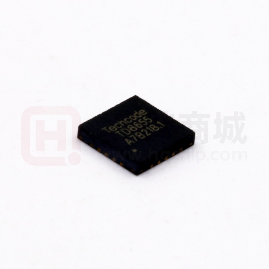
TD8655
40Vin 4 Outputs Buck Controller
General Description
Features
TD8655 is a DC/DC Buck Synchronous with four current limit
pins suitable for many multi‐output applications. It is
designed to allow for operating a wide supply voltage range
from 9V to 40V. It has both high‐side and low‐side drivers
allowing synchronous configuration using two external
power‐NMOS. This IC can operate in both Constant Current
(CC) and Constant Voltage (CV) modes.
TD8655 operates as a DC‐DC Buck Controller providing a wide
range of outputs at Constant Current (CV) from 1.2V to 28V
and the output current as high as 10A or above. It has a
Constant Current(CC) mode so that output current can be set
externally and at a accuracy of +/‐7%.
The current mode control and external compensation makes
feedback control have good line and load regulation with
flexible external design.
There are four independent current limit control pins for four
separate loads. Each of the current limit can be set by a
resistor(RCS) at 100mV across it. Of course, output peak
current limit is working during normal operation
Vin: 8.5V to 40V
Vout: 1.2V to 28V; typical at 5V
CC/CV Mode Control
PFM Mode for Increased Light Load Efficiency
4 outputs current precision OCP: Adjustable
Current‐Limit Protection
Burst mode when OCP/SCP occur
Protection
NMOS peak current limit: accuracy:~10%
Output short protection: reduce input current to
less than 20mA(RMS)
OVP(output Over‐Voltage Protection)
Output FB short protection
Temperature shut down(OTP)
Adjustable Output Cable Resistance Compensation
Duty: 0~97%
Switching Frequency: 100kHz to 300KHz
Integrated MOSFET Drivers
QFN20 Package
Applications
Pin Configurations
Car Charger
High‐Brightness Lighting
General‐Purpose DC/DC Controller
Figure1 Pin Configuration of TD8655(Top View)
April, 13, 2016. Techcode Semiconductor Limited www.techcodesemi.com
1
�
Techcode®
40Vin 4 Outputs Buck Controller
DATASHEET
TD8655
Pin Description
Pin Number
Pin Name
Description
1
BST
Internal High Side Driver Power Bias which is typically 5V above Vin. A typical 0.1uF
capacitor is used connecting between BST and SW pins.
2
VIN
Supply input
3
ISENSE
Input Current Sense, the sense Resistor must be >5mohm.
4
COMP
Error Amplifier Output and the Converter stability compensation network is placed.
5
FREQ
Switching Frequency setting.
6
FB
Feedback input with reference to 1.20V. it can sets output voltage.
7
En
On/off control pin
8
ISET
To set output constant current.
9
COUT1
Current limit of the 1st output. The Threshold voltage is 100mV.
10
COUT2
Current limit of the 2nd output. The Threshold voltage is 100mV.
11
COUT3
Current limit of the 3rd output. The Threshold voltage is 100mV.
12
COUT4
Current limit of the 4th output. The Threshold voltage is 100mV.
13
CS34
Pull low to disable COUT3/COUT4 CC function and high to enable.
14
SS
Soft start pin. a capacitor is connected between this pin and GND
15
TS
Test pin
16
GND
Ground pin.
17
LSD
Low Side Driver
18
VDD
Internal 5v power supply, a 1uF (or more) capacitor is connected between this pin and GND.
19
SW
Inductor terminal.
20
HSD
High Side Driver
April, 13, 2016. Techcode Semiconductor Limited www.techcodesemi.com
2
�Techcode®
DATASHEET
TD8655
40Vin 4 Outputs Buck Controller
Function Block
Figure 2 Function Block Diagram of TD8655
Absolute Maximum Ratings
Symbol
Parameter
VIN
Supply Input Voltage
Rating
‐0.3 to +43
Unit
ISNESE to GND
‐0.3 to VIN
V
BS to SW
‐0.3 to +6
V
SW to GND
‐1 to VIN+1
V
BS, HSD to GND
VSW‐0.3 to VSW+6
V
VFB,ISET,COMP,LSD,COUT1‐4,FREQ,SS CS34,TS to GND
‐0.3 to +6
V
ESD
HBM (Human Body Mode)
2K
V
θJA
Thermal Resistance from Junction to ambient
40
ºC/W
V
April, 13, 2016. Techcode Semiconductor Limited www.techcodesemi.com
3
�Techcode®
DATASHEET
TD8655
40Vin 4 Outputs Buck Controller
Recommended Operating Conditions
Symbol
Parameter
Rating
Min.
Typ.
Max.
VIN
Supply Voltage
9
‐
40
V
VOUT
Output voltage range
1.2
‐
28
V
IOUT
Output current range
‐
‐
15
A
Operating Temperature
‐40
85
ºC
TSTG
Storage Temperature Range
‐60
150
ºC
TSDR
Maximum Lead Soldering Temperature, 10 Seconds
260
Unit
ºC
Electrical Characteristics
(VIN=12V, TA=25°C (unless otherwise specified). MOSFET use TDM3436)
Symbol
VIN
Characteristic
Test conditions
Min
Supply Voltage
9
IIN
Supply Input Current
EN=3V, Vout=5V,No load
IQ
Shutdown Supply Current
VUP
VHYS
Typ
Max
Unit
40
V
1
1.7
2.5
mA
EN=0
‐
‐
30
uA
VIN UVLO Turn ON
VIN Rising
8.2
8.5
8.9
V
VIN UVLO Hysteresis
VIN Falling
‐
1.0
‐
V
VIN UVLO
Feedback voltage
VFB
Feedback voltage
VEN=3V
1.176
1.20
1.224
V
Tolerance
‐2
‐
2
%
FSW
Switch frequency
RFREQ=60Kohm
170
200
230
KHz
TON
Minimum On‐Time
‐
150
‐
ns
D
Duty cycle
‐
‐
99
%
VTOCP
OCP threshold
95
100
105
mV
IFB
Cable compensation Current
Cout1‐4=100mv
‐
40
‐
uA
Oscillator
Current sense
HDR & LDR Drivers
TRH
HDR Rising Time
‐
10
‐
ns
TFH
HDR Falling Time
‐
10
‐
ns
TRL
LDR Rising Time
‐
10
‐
ns
TFL
LDR Falling Time
‐
10
‐
ns
TLH
Dead Time
‐
80
‐
ns
THL
Dead Time
‐
80
‐
ns
April, 13, 2016. Techcode Semiconductor Limited www.techcodesemi.com
4
�Techcode®
DATASHEET
TD8655
40Vin 4 Outputs Buck Controller
Soft start
TSS
Soft start time
CSS =0.1uF
10
ms
Thermal Shutdown(OTP)
TSD
Temperature Rising
‐
150
‐
ºC
THYS
OTP Hysteresis
‐
20
‐
ºC
April, 13, 2016. Techcode Semiconductor Limited www.techcodesemi.com
5
�Techcode®
DATASHEET
TD8655
40Vin 4 Outputs Buck Controller
Typical Application Circuit1
Vin
VIN
VOUT
C1
R6
0.005
C2
10uF
EC1
0.1uF
Output1
100uF
U1
2
CS1
VIN
R10
R18
R19
5
GND
39K 1%
ISENSE
HSD
C13
4
R5
220pF
4
2.2R
3
1
2
1
0.1uF
SW
C15
22pF
TD8655
LSD
R7
7
R9
COMP
1M
VIN
20
C10
ISET
BST
GND
GND
EN
COUT1
R8
2.2R
17
4
9
R17
300
CS1
2
1
1uF
VDD
GND
COUT2
S
D
TDM3436
S
S
D
D
D
5
GND
VOUT
6
7
Output2
CS2
8
L1
R20
300
10
G
S TDM3436
D
S
D
S
Q2
CS2
D
D
5
470uF/10V
GND
EC2
CS34
R4
0.1uF
7
10.5K/1%
Output3
CS3
GND
GND
R2
3.3K/1%
11
R21
300
SS
CS3
GND
C20
TS
VOUT
6
FB
GND
GND
16
0.1uF
R14
0.04/1%
GND
COUT3
1uF
15
C3
VOUT
8
1uF
14
GND
C5
6
C19
13
R13
0.04/1%
VOUT
22uH
C22
C12
1uF
G
Q1
19
3
1M
18
R12
0.04/1%
20
FREQ
20K 1%
8
3
COUT4
12
R22
300
C21
GND
Output4
CS4
CS4
1uF
R15
0.04/1%
GND
GND
GND
Fig3 4‐outputs with OCP(CS1~4) and CC(CS1+CS2+CS3+CS4)
April, 13, 2016. Techcode Semiconductor Limited www.techcodesemi.com
6
�Techcode®
DATASHEET
TD8655
40Vin 4 Outputs Buck Controller
Typical Application Circuit2
Vin
VIN
VOUT
C1
R6
0.005
C2
10uF
EC1
0.1uF
Output1
100uF
U1
2
CS1
VIN
R10
R18
R19
5
GND
39K 1%
ISENSE
HSD
R5
C13
4
ISET
C15
22pF
TD8655
LSD
R7
7
4
3
1
2
1
EN
COUT1
17
R17
300
9
VDD
4
CS1
2
1
GND
COUT2
S
D
TDM3436
D
S
D
S
D
GND
5
6
7
8
L1
VOUT
22uH
R8
2.2R
C22
1uF
C12
1uF
G
Q1
19
3
1M
18
2.2R
0.1uF
SW
VIN
R9
COMP
1M
220pF
20
C10
BST
GND
G
D
S TDM3436
D
S
D
S
D
C5
R4
0.1uF
10.5K/1%
7
VOUT
8
Output2
CS2
GND
GND
R2
3.3K/1%
R21
300
11
CS2
GND
C20
1uF
TS
GND
FB
15
COUT3
SS
GND
14
R14
0.04/1%
CS34
COUT4
GND
12
16
6
13
0.1uF
EC2
6
Q2
10
470uF/10V
5
GND
C3
R12
0.04/1%
FREQ
20K 1%
8
GND
20
3
GND
Fig4 2‐outputs with OCP and CC(CS1+CS2)
April, 13, 2016. Techcode Semiconductor Limited www.techcodesemi.com
7
�Techcode®
DATASHEET
TD8655
40Vin 4 Outputs Buck Controller
Typical Application Circuit3
Vin
VIN
C1
R6
0.005
C2
10uF
EC1
0.1uF
U1
2
100uF
VIN
R10
R18
R19
5
GND
39K 1%
ISENSE
HSD
C13
4
R5
220pF
SW
TD8655
LSD
R7
3
1
2
1
COUT1
19
17
9
VDD
4
R17
300
CS1
2
1
GND
COUT2
S
D
TDM3436
D
S
D
S
D
7
8
L1
VOUT
G
D
S TDM3436 D
S
D
S
D
Q2
10
Output1
5
CS1
470uF/10V
C5
6
EC2
R4
0.1uF
7
R12
0.02/1%
10.5K/1%
8
GND
GND
GND
R2
3.3K/1%
COUT3
11
SS
TS
GND
16
FB
15
CS34
COUT4
12
6
14
GND
13
0.1uF
6
VOUT
GND
C3
5
22uH
R8
2.2R
C22
1uF
C12
1uF
G
Q1
3
EN
1M
18
4
2.2R
0.1uF
C15
22pF
7
R9
COMP
1M
VIN
20
C10
ISET
BST
GND
GND
20
FREQ
20K 1%
8
3
GND
Fig5 1 output with CC.
April, 13, 2016. Techcode Semiconductor Limited www.techcodesemi.com
8
�
Techcode®
DATASHEET
TD8655
40Vin 4 Outputs Buck Controller
Function Description
TD8655 operates in a peak‐current–mode control to regulate
the output voltage. The internal clock initiates the PWM
cycle, which turns on the integrated high side power
MOSFET. The high‐side MOSFET remains on until its current
reaches the value set by the COMP voltage. When the power
switch is off, it remains off until the next clock cycle begins.
current can be calculated by followings:
ICC = VISET/(10*(RCS1// RCS2//RCS3//RCS4))
Here VISET=1.2V*(R18/(R18+R19)), R18 and R19 refer to
Typical Application Circuit, RCS1,2,3,4 are the sense resistors
between COUT1,2,3,4 and GND.
Output Cable Resistance Compensation
CC/CV Mode Control
R1 will can program the cable compensation.
To compensate for resistive voltage drop across the charger's
output cable, the TD8655 integrates a simple,
user‐programmable cable voltage drop compensation using
the impedance at the FB pin. By choosing different R1,we can
get different cable voltage drop compensation values. The
compensation voltage(Vdelta) can be calculated by:
Vdelta=IFB*R1=R1*(VCS1+VCS2+VCS3+VCS4)/10K.
VCS1/CS2/CS3/CS4 are the voltages on the pins Cout1‐4. R1 is the
resistor between VFB and VOUT.
Over Current limit setting
A drop voltage on the current sensing resister is over the OCP
value, the controller will enter hiccup mode. The Current limit
is set by outside resistance (RSENSE), When the cout1 or cout2
or cout3 or cout4 voltage larger than 100mV, the current
limit occurs. The Output current limit(IOC) set according to the
following equation:
IOC=100mv/RCS
Over Temperature Protection (OTP)
TD8655 provides over temperature protection(OTP) . The
OTP will shut down the converter when junction temperature
exceeds 150°C. Once the junction temperature cools down by
approximately 20°C, the controller will resume.
Constant Current setting:
Frequency setting
TD8655 provides CC/CV function. The Constant output
Current control Mode and Constant output Voltage control
Mode.
Output Voltage Setting
VFB is the feedback pin and connected to the non‐inverting
of error amplifier input. The output voltage is adjustable from
1.2V to 28V with a resistor‐divider connected with VFB
GND and converter’s output. Using 1% or better resistors for
the resistor‐divider is recommended.
The output voltage is determined by the equation:
VOUT=VFB*(1+R1/R2)=1.2V*(1+R1/R2)
At this time Cout1‐4 should be lower than the OCP threshold The FREQ pin is used to set the operation frequency and a
(100mv). The sum voltage of Cout1‐4 pins reaches the 120k~30k ohm resistor is connected FREQ pin and GND. The
frequency is decided by the equation: FSW=12000k/RF, RF is
voltage on VISET pin, the system will enter CC mode, the CC
the resistor between this pin and GND with unit in kohm.
April, 13, 2016. Techcode Semiconductor Limited www.techcodesemi.com
9
�Techcode®
DATASHEET
TD8655
40Vin 4 Outputs Buck Controller
If this pin is floating, the frequency is 200khz.
Output Inductor Selection
The inductor value (L) determines the inductor ripple current,
IRIPPLE and affects the load transient response. Higher
inductor value reduces the inductor’ s ripple current and
induces lower output ripple voltage. The ripple current and
ripple voltage can be approximated by:
L=VOUT*(VIN‐VOUT)/FSW*IRIPPLE*VIN
Where
FSW : the switching frequency of the regulator; VIN/VOUT :
input voltage/output voltage;
IRIPPLE is the inductor ripple current and IRIPPLE=(0.3‐0.5)IOUT
Input Capacitor
A low ESR capacitor is highly recommended. Since large
current flows in and out of this capacitor during switching, its
ESR also affects efficiency.
The input capacitance should be higher than 100μF. The best
choice is the ceramic type, however, low ESR tantalum or
electrolytic types may also be used. The input capacitor
should be placed close to the VIN and GND pins of the IC,
with the shortest traces possible. In the case of tantalum or
electrolytic types, they can be further away if a small parallel
1μF ceramic capacitor is placed right next to the IC.
Output Capacitor
The system requires the output capacitor to maintain the dc
output voltage. The characteristics of the output capacitor
affect the stability of the regulatory system. A low ESR
electrolytic capacitor is recommended for a low output ripple
and good control loop stability. For general applications, a 1µF
ceramic capacitor and a 330µF (or more) polymer/electrolytic
capacitor are recommended.
April, 13, 2016. Techcode Semiconductor Limited www.techcodesemi.com
10
�Techcode®
DATASHEET
TD8655
40Vin 4 Outputs Buck Controller
Package Information
QFN20L Package Outline Dimensions
Symbol
A
A1
b
c
D
D2
MIN
0.7
‐
0.18
0.18
3.90
2.55
Millimeter NOM
0.75
0.02
0.25
0.20
4.00
2.65
MAX
0.8
0.05
0.30
0.25
4.10
2.75
e
Ne
Nd
0.50
BSC
2.00
BSC
2.00
BSC
E
E2
L
h
3.90
2.55
0.35
0.30
4.00
2.65
0.40
0.35
4.10
2.75
0.45
0.40
April, 13, 2016. Techcode Semiconductor Limited www.techcodesemi.com
11
�
Techcode®
DATASHEET
TD8655
40Vin 4 Outputs Buck Controller
Design Notes
April, 13, 2016. Techcode Semiconductor Limited www.techcodesemi.com
12
�