IPT2601
FINE MAD ELECTRONICS GROUP
USB Dedicated Fast-Charging Port Controller
1 FEATURES
Support HiSilicon® Fast Charge
Protocol(FCP)
Support Samsung® Adaptive Fast
Charging(AFC)
Support Qualcomm® Quick Charging
3.0/2.0(QC3.0/QC2.0)™ Protocol
Support USB DCP applying 2.7V on DP
and DM line, output Current up to 2.4A
for Apple® Device
Meets Battery Charging Specification BC
1.2 for DCP
Meets Chinese Telecommunication
Industrial Standard YD/T 1591-2009
Automatic Selection of D+/D- mode for
an attached device
Power Consumption below 1mW at 5V
output
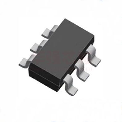
SOT23-6 Package
Adapter
Car Charger
USB Power Output Ports
Power Bank
3 DESCRIPTION
IPT2601 is a low-cost USB Dedicated Fast
Charging Port Controller which is fully
compatible with BC1.2 and other non BC1.2
standards like YD/T 1591-2009 Apple® &
Samsung® Charging Spec, HiSilicon® Fast
Charge Protocol, Qualcomm® Quick
Charging™ 3.0/2.0.
IPT2601 automatically detect whether a
connected Power Device(PD) is Quick
Charge 2.0/3.0 or FCP Capable before
enabling output voltage adjustment. If a PD
not compliant to Quick Charge 2.0/3.0 is
detected the IPT2601 disables output
voltage adjustment to ensure safe
operation with legacy 5V only USB PDs.
The IPT2601 is available in SOT23-6
package.
2 APPLICATIONS
VBUS
D-
2.2K
D+
100K
Feedback
Node
1u
VDD
DM
FBO
DP
QC_EN
GND
USB Connector
4 Typical Application Schematic
GND
IPT2601
1
www.superchip.cn
No: S&CIC1487
Copyright © 2017, FINE MAD ELECTRONICS GROUP
�IPT2601
FINE MAD ELECTRONICS GROUP
5 PIN FUNCTIONS
DP
1
6
DM
GND
2
5
VDD
FBO
3
4
QC_EN
IPT2601
NO.
1
NAME
DP
TYPE
I/O
DESCRIPTION
2
GND
P
3
FBO
Feedback output. Current source/sink output.
4
QC_EN
I/O
I
5
VDD
Power supply.
6
DM
P
I/O
USB positive data line.
Ground connection.
FCP/QC function enable, H-z to enable FCP/QC and LOW to disable.
USB negative data line.
6 SPECIFICATIONS
6.1 ABSOLUTE MAXIMUM RATINGS (1)
PARAMETER
MIN
MAX
UNIT
VDD
-0.3
6.5
V
Others
-0.3
6.5
V
Operating Junction Temperature
TJ
-40
150
Storage Temperature Range
TSTG
-65
150
Voltage Range(To PGND)
(1) Stresses beyond those listed under Absolute Maximum Ratings may cause permanent damage to the
device. Exposure to absolute-maximum-rated conditions for extended periods may affect device
reliability.
6.2 ESD RATING
SYMBOL
VESD
PARAMETER
VALUE
UNIT
Human Body Model (HBM)
±4000
V
6.3 RECOMMENDED OPERATING CONDICTIONS
PARAMETER
MIN
TYP
MAX
UNIT
5
6.4
V
VDD
Input Supply Voltage
3.2
CVDD
Input Capacitance
0.47
TA
Operation Temperature Range
-40
2
www.superchip.cn
No: S&CIC1487
µF
85
Copyright © 2017, FINE MAD ELECTRONICS GROUP
�IPT2601
FINE MAD ELECTRONICS GROUP
6.4 ELECTRICAL CHARACTERISTICS
Conditions are
.
TEST
CONDICTIONS
PARAMETER
MIN
TYP
MAX
UNIT
5.5
V
INPUT POWER
VVDD
VDD Input Voltage Range
3.2
IVDD
VDD Supply Current
VDD=5V
200
uA
VVDD(SHUNT)
VDD Shunt Voltage
IVDD=3.5mA
4.75
V
VDD(ON)
VDD (turn on threshold voltage)
VVDD Rising
2.9
3.0
3.1
V
VDD(OFF)
VDD (turn off threshold voltage)
VVDD Falling
2.8
2.9
3.0
V
ΔVUVLO
UVLO Hysteresis
VDD(ON)- VDD(OFF)
VDD UVLO Test
0.1
V
High Voltage Dedicated Charging Port (HVDCP)
VDAT(REF)
TGLITCH(DP)HIGH
Data Detect Voltage
Output voltage selection
reference
D+ High Glitch Filter Time
TGLITCH(DM)LOW
D- Low Glitch Filter Time
TGLITCH(V)CHANGE
Output Voltage Glitch Filter Time
Continuous Mode Glitch Filter
Time
VSEL(REF)
TGLITCH(CONT)CHANGE
0.25
0.325
0.4
V
1.8
2
2.2
V
1
1.25
1.5
s
1
VDD=3.1-7V,
V(D+)=0.5-3.6V,
Switch SW1=Off
ms
20
40
60
ms
100
150
200
us
300
500
800
KΩ
14.2
19.5
24.5
KΩ
20
40
Ω
1
nF
RDAT(LKG)
D+ Leakage Resistance
RDM(DWN)
D- Pull-Down Resistance
RON(N1)
Switch SW1 on-resistance
CDAT
ΔIT(UP)
Data Line Capacitance
Output Device Connection
Detection threshold
Output Device connection
Detection Glitch Filter Time
Up Current Step
RIREF=100KΩ
2
uA
ΔIT(DO)
Down Current Step
RIREF=100KΩ
2
uA
TDUR(step)
Duration for current step
QC3.0 mode
VTH(PD)
TDPD
VDD=3.1-7V,
V(D+)≤3.6V,
IDRAIN=200uA
0.25
0.325
0.4
V
120
160
200
ms
80
100
120
us
1.08
1.2
1.32
V
DCP 1.2V Mode
VDAT(1.2V)
RDAT(1.2V)
D+_1.2V/D-_1.2V line output
voltage
D+_1.2V/D-_1.2V line output
Impedance
100
KΩ
Apple 2.4A Mode
3
www.superchip.cn
No: S&CIC1487
Copyright © 2017, FINE MAD ELECTRONICS GROUP
�IPT2601
FINE MAD ELECTRONICS GROUP
VDAT(2.7V)
D+/D- line output voltage
RDAT(2.7V)
D+/D- line output Impedance
2.57
2.7
2.84
33.6
V
KΩ
FCP Mode
VTX-VOH
D- FCP TX Valid High
VTX-VOL
D- FCP TX Valid Low
VRX-VIH
D- FCP RX Valid High
VRX-VIL
D- FCP RX Valid High
RPD
D- Pull-Down Resistance
TUI
Unit Interval for PHY
FCLK=125KHz
TRISE
FCP Pulse Rise Time
TFALL
FCP Pulse Fall Time
4
www.superchip.cn
No: S&CIC1487
2.35
1.5
3.6
V
0.3
V
3.6
V
1.0
V
400
500
600
Ω
144
160
176
us
10% - 90%
1
2.5
us
90% - 10%
1
2.5
us
Copyright © 2017, FINE MAD ELECTRONICS GROUP
�IPT2601
FINE MAD ELECTRONICS GROUP
7 Outline Information
Symbol
A
A1
A2
b
c
D
E
E1
e
e1
L
5
www.superchip.cn
Dimensions In Millimeters
Min
Max
1.050
1.250
0.000
0.100
1.050
1.150
0.300
0.500
0.100
0.200
2.820
3.020
1.500
1.700
2.650
2.950
0.950
1.800
2.000
0.300
0.600
0°
8°
No: S&CIC1487
Dimensions In Inches
Min
Max
0.041
0.049
0.000
0.004
0.041
0.045
0.012
0.020
0.004
0.008
0.111
0.119
0.059
0.067
0.104
0.116
0.037
0.071
0.079
0.012
0.024
0°
8°
Copyright © 2017, FINE MAD ELECTRONICS GROUP
�
很抱歉,暂时无法提供与“IPT2601”相匹配的价格&库存,您可以联系我们找货
免费人工找货