GS393/393A
LOW POWER LOW OFFSET VOLTAGE DUAL COMPARATORS
Features
Wide Supply Voltage Range
Differential Input Voltage Range Equals to the
Single Supply: 2.0V to 36V
Power Supply Voltage
Dual Supplies: ±1.0V to ±18V
Low Output Saturation Voltage: 200mV at 4mA
Low Supply Current Drain: 0.6mA
Open Collector Output
Low Input Bias Current: 25nA (Typical)
Small Package:
Low Input Offset Current: ±5.0nA (Typical)
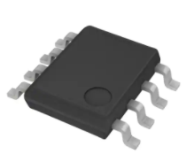
GS393/393A Available in SOP-8 and DIP-8 Packages
Low Input Offset Voltage: 1.0mV (Typical)
Input Common Mode Voltage Range Includes
Ground
General Description
The GS393/393A consist of two independent precision voltage comparators with a typical offset voltage of 1.0mV
and high gain. They are specifically designed to operate from a single power supply over wide range of voltages.
Operation from split power supply is also possible and the low power supply current drain is independent of the
magnitude of the power supply voltage.The GS393/393A series are compatible with industry standard 393. GS393A
has more stringent input offset voltage than GS393.
Applications
Battery Charger
DC-DC Module
Cordless Telephone
PC Motherboard
Switching Power Supply
Communication Equipment
Pin Configuration
Figure 1. Pin Assignment Diagram
Functional Block Diagram
Figure 2. Functional Block Diagram of GS393/393A (Each comparator)
V0
1/8
�GS393/393A
Absolute Maximum Ratings
Condition
Symbol
Max
Vcc
±20V or 40V
VI(DIFF)
40V
VI
-0.3V~40V
Operating Temperature Range
Topr
-25°C ~+125°C
Storage Temperature Range
Tstg
-65°C ~+150°C
Power Supply Voltage
Differential input voltage
Input Voltage
Note 1: Stresses greater than those listed under "Absolute Maximum Ratings" may cause permanent damage to the device.
These are stress ratings only, and functional operation of the device at these or any other conditions beyond those indicated
under "Recommended Operating Conditions" is not implied. Exposure to "Absolute Max-imum Ratings" for extended periods may
affect device reliability.
Note 2: This input current will only exist when the voltage at any of the input leads is driven negative. It is due to the
collector-base junction of the input PNP transistors becoming forward biased and thereby acting as input diode clamps. In
addition to this diode action, there is also lateral NPN parasitic transistor action on the IC chip. This transistor action can cause
the output voltages of the comparators to go to the V+ voltage level (or to ground for a large overdrive) for the time duration that
an input is driven negative. This is not destructive and normal output states will re-establish when the input voltage, which was
negative, again returns to a value greater than -0.3 VDC at 25°C).
Package/Ordering Information
MODEL
CHANNEL
GS393
Dual
GS393A
Dual
V0
PACKAGE
PACKAGE
MARKING
DESCRIPTION
OPTION
INFORMATION
GS393-SR
SOP-8
Tape and Reel,4000
GS393
GS393-DR
DIP-8
20Tube(1000pcs)
GS393
GS393A-SR
SOP-8
Tape and Reel,4000
GS393
GS393A-DR
DIP-8
20Tube(1000pcs)
GS393
ORDER NUMBER
2/8
�GS393/393A
Recommended Operating Conditions
Electrical Characteristics
o
o
o
Limits in standard typeface are for TA=25 C, bold typeface applies over TA=-40 C to 85 C (Note 3), VCC=5V, GND=0V, unless
otherwise specified.
o
≤ TA ≤85
Note 3: These specifications are limited to -40 C
o
C. Limits over temperature are guaranteed by design, but not
tested in production.
Note 4: The input common-mode voltage of either input signal voltage should not be allowed to go negatively by
o
o
more than 0.3V (at 25 C). The upper end of the common-mode voltage range is VCC-1.5V (at 25 C), but either or
both inputs can go to +36V without damages,
V0
independent of the magnitude of the VCC.
3/8
�GS393/393A
Typical Performance characteristics
V0
4/8
�GS393/393A
Typical Performance characteristics
V0
5/8
�GS393/393A
Typical Applications
V0
6/8
�GS393/393A
Package Information
SOP-8
V0
7/8
�GS393/393A
DIP-8
V0
8/8
�
很抱歉,暂时无法提供与“GS393A-SR”相匹配的价格&库存,您可以联系我们找货
免费人工找货