物料型号:GS393/393A
器件简介:
GS393/393A是一款低功耗、低偏移电压的双比较器,具有2.0V至36V的宽电源电压范围,以及±1.0V至±18V的双电源电压范围。它们设计用于在宽电压范围内从单电源供电操作,也可以从分电源供电操作,而低电源电流消耗与电源电压的大小无关。GS393/393A系列与行业标准的393兼容,GS393A具有比GS393更严格的输入偏移电压。
引脚分配:
- OUTA1: 输出A1
- INA-2: 输入A-
- INA+3: 输入A+
- OUTB: 输出B
- INB: 输入B-
- VSS4: 地
- 5INB+: 输入B+
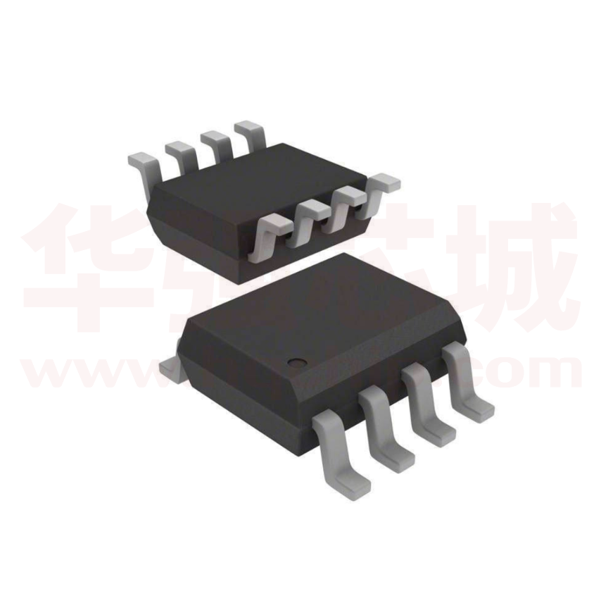
- SOP-8和DIP-8封装
参数特性:
- 低输出饱和电压:4mA时为200mV
- 低电源电流消耗:0.6mA
- 开集电极输出
- 低输入偏置电流:典型值为25nA
- 小型封装:SOP-8和DIP-8
- 低输入偏移电流:典型值为±5.0nA
- 输入共模电压范围包括地
功能详解:
GS393/393A包含两个独立的精密电压比较器,具有1.0mV的典型偏移电压和高增益。它们特别设计用于在宽电压范围内从单电源供电。分电源供电也是可能的,并且低电源电流消耗与电源电压的大小无关。GS393A与GS393相比,具有更严格的输入偏移电压。
应用信息:
- 电池充电器
- DC-DC模块
- 无绳电话
- 电脑主板
- 开关电源
- 通信设备
封装信息:
- GS393: 双通道,SOP-8封装,订购号GS393-SR,DIP-8封装,订购号GS393-DR
- GS393A: 双通道,SOP-8封装,订购号GS393A-SR,DIP-8封装,订购号GS393A-DR