物料型号:74HC02
器件简介:74HC02 是一个由四个独立的 2 输入正逻辑与非门(NAND)组成的集成电路。
引脚分配:1-Vcc,2-A1,3-B1,4-Y1,5-GND,6-B2,7-A2,8-Y2,9-GND,10-A3,11-B3,12-Y3,13-GND,14-B4,15-A4,16-Y4。
参数特性:工作电压范围 2V 到 6V,工作电流低,逻辑电平 NO 和 NC 分别代表逻辑 1 和 0。
功能详解:每个与非门有两个输入端和一个输出端,输出低电平表示两个输入端至少有一个是高电平。
应用信息:广泛应用于数字逻辑电路设计中,如构成触发器、寄存器、计数器等。
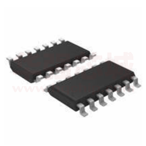
封装信息:通常采用双列直插式封装(DIP)或表面贴装封装(SMD)。