WST6004
N-Ch MOSFET
General Description
Product Summery
The WST6004 is the highest performance trench
N-Ch MOSFET with extreme high cell density ,
which provide excellent RDSON and gate
charge for most of the small power switching and
load switch applications.
BVDSS
RDSON
ID
20V
140mΩ
0.6A
Applications
The WST6004 meet the RoHS and Green
Product requirement with full function
reliability approved.
Replace Digital Transistor
Power Supply Converter Circuits
Load/Power Switching Cell Phones, Pagers
Features
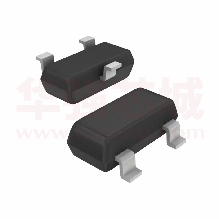
SOT-523 Pin Configuration
High-speed switching
D
Green Device Available
3
1
2
G
S
Absolute Maximum Ratings
Symbol
Parameter
Rating
Units
VDS
Drain-Source Voltage
20
V
VGS
Gate-Source Voltage
±8
V
ID@TA=25℃
Continuous Drain Current, VGS @ 10V1
600
mA
ID@TA=70℃
Continuous Drain Current, VGS @ 10V1
300
mA
3
A
IDM
Pulsed Drain Current
2
3
PD@TA=25℃
Total Power Dissipation
0.175
W
TSTG
Storage Temperature Range
-55 to 150
℃
TJ
Operating Junction Temperature Range
-55 to 150
℃
Thermal Data
Symbol
RθJA
www.winsok.tw
Parameter
Thermal Resistance Junction-Ambient
Page 1
1
Typ.
Max.
Unit
---
625
℃/W
Dec.2014
�WST6004
N-Ch MOSFET
Electrical Characteristics (TJ=25 ℃, unless otherwise noted)
Symbol
BVDSS
Parameter
Conditions
Drain-Source Breakdown Voltage
△BVDSS/△TJ BVDSS Temperature Coefficient
RDS(ON)
Static Drain-Source On-Resistance2
VGS(th)
Gate Threshold Voltage
Min.
Typ.
Max.
Unit
20
---
---
V
---
0.05
---
V/℃
---
140
450
---
180
765
0.35
---
1.0
V
---
-3.7
---
mV/℃
VDS=16V , VGS=0V , TJ=25℃
---
---
1
VDS=16V , VGS=0V , TJ=55℃
---
---
5
=
VGS=0V , ID 250uA
Reference to 25℃ , ID=1mA
=
VGS=4.5V , ID 0.6A
=
VGS=2.5V , ID 0.5A
VGS=VDS , ID =250uA
mΩ
△VGS(th)
VGS(th) Temperature Coefficient
IDSS
Drain-Source Leakage Current
IGSS
Gate-Source Leakage Current
VGS=±8V , VDS=0V
---
---
±10
uA
gfs
Forward Transconductance
VDS=5V=
, ID 0.1A
---
880
---
mS
---
6
---
---
3.8
---
---
28
---
Fall Time
---
18
---
Ciss
Input Capacitance
---
130
---
Coss
Output Capacitance
---
20
---
Crss
Reverse Transfer Capacitance
---
16
---
Min.
Typ.
Max.
Unit
---
---
100
mA
---
---
0.5
A
---
---
1
V
Td(on)
Tr
Td(off)
Tf
Turn-On Delay Time
VDD=15V , VGS=10V ,
Rise Time
RG=3.3Ω, ID=0.1A
Turn-Off Delay Time
VDS=15V , VGS=0V , f=1MHz
uA
ns
pF
Diode Characteristics
Symbol
IS
ISM
VSD
Parameter
Conditions
1,4
Continuous Source Current
2,4
Pulsed Source Current
2
Diode Forward Voltage
VG=VD=0V , Force Current
VGS=0V , IS=0.2A , TJ=25℃
Note :
2
1.The data tested by surface mounted on a 1 inch FR-4 board with 2OZ copper.
2.The data tested by pulsed , pulse width ≦ 300us , duty cycle ≦ 2%
3.The power dissipation is limited by 150℃ junction temperature.
4.The data is theoretically the same as ID and IDM , in real applications , should be limited by total power dissipation.
www.winsok.tw
Page 2
Dec.2014
�WST6004
N-Ch MOSFET
Typical Performance Characteristics
Output Characteristics
Transfer Characteristics
5.0
4.5
4.0
VGS=4V,5V
Ta=25℃
VDS=3V
VGS=3V
3.5
VGS=2.5V
3.0
Pulsed
Pulsed
3.0
DRAIN CURRENT
DRAIN CURRENT
ID
ID
(A)
3.5
(A)
4.0
VGS=2V
2.5
2.0
1.5
Ta=100℃
2.0
1.5
0.5
0.5
0.0
0.0
Ta=25℃
1.0
VGS=1.5V
1.0
2.5
0.5
1.0
1.5
2.0
2.5
3.0
3.5
DRAIN TO SOURCE VOLTAGE
4.0
VDS
4.5
0.0
5.0
0
(V)
1
2
3
GATE TO SOURCE VOLTAGE
VGS
4
(V)
RDS(ON) —— VGS
RDS(ON) —— ID
500
800
Pulsed
Ta=25℃
700
350
(m)
400
VGS=2.5V
300
VGS=4.5V
500
250
200
0.1
ID=0.65A
600
ON-RESISTANCE
ON-RESISTANCE
RDS(ON)
(m)
VGS=1.8V
RDS(ON)
450
Pulsed
Ta=100℃
400
300
Ta=25℃
200
0.2
0.3
0.4
0.5
0.6
0.7
DRAIN CURRENT
0.8
ID
0.9
1.0
1.1
100
1.2
1
(A)
2
3
4
GATE TO SOURCE VOLTAGE
GS
5
(V)
Threshold Voltage
IS —— VSD
2
0.8
Pulsed
1
VTH
0.1
Ta=100℃
THRESHOLD VOLTAGE
SOURCE CURRENT
IS (A)
(V)
0.7
Ta=25℃
0.6
ID=250uA
0.5
0.4
0.3
0.01
0.0
0.2
0.4
0.6
0.8
1.0
SOURCE TO DRAIN VOLTA
VOLTAGE
www.winsok.tw
1.2
SD
1.4
1.6
0.2
25
(V)
50
75
JUNCTION TEMPERATURE
Page 3
100
Tj
125
(℃ )
Dec.2014
�WST6004
N-Ch MOSFET
627�����3DFNDJH�2XWOLQH�'LPHQVLRQV�
Symbol
A
A1
A2
b1
b2
c
D
E
E1
e
e1
L
L1
Κ
Dimensions In Millimeters
Min.
Max.
0.700
0.900
0.000
0.100
0.700
0.800
0.150
0.250
0.250
0.350
0.100
0.200
1.500
1.700
0.700
0.900
1.450
1.750
0.500 TYP.
0.900
1.100
0.400 REF.
0.260
0.460
0°
8°
Dimensions In Inches
Min.
Max.
0.028
0.035
0.000
0.004
0.028
0.031
0.006
0.010
0.010
0.014
0.004
0.008
0.059
0.067
0.028
0.035
0.057
0.069
0.020 TYP.
0.035
0.043
0.016 REF.
0.010
0.018
0°
8°
627���� 6XJJHVWHG�3DG�/D\RXW
�
www.winsok.tw
Page 4
Dec.2014
�Attention�
1,�Any�and�all�Winsok�power�products�described�or�contained�herein�do�not�have�specifications�that�can�handle�
applications�that�require�extremely�high�levels�of�reliability,�such�as�lifeͲsupport�systems,�aircraft's�control�systems,�or�
other�applications�whose�failure�can�be�reasonably�expected�to�result�in�serious�physical�and/or�material�damage.� �
Consult�with�your�Winsok�power�representative�nearest�you�before�using�any�Winsok�power�products�described�or�
contained�herein�in�such�applications.�
2,Winsok�power�assumes�no�responsibility�for�equipment�failures�that�result�from�using�products�at�values�that�exceed,� �
even�momentarily,�rated�values�(such�as�maximum�ratings,�operating�condition�ranges,�or�other�parameters)�listed�in�
products�specifications�of�any�and�all�Winsok�power�products�described�or�contained�herein.�
3,�Specifications�of�any�and�all�Winsok�power�products�described�or�contained�herein�stipulate�the�performance,�
characteristics,�and�functions�of�the�described�products�in�the�independent�state,�and�are�not�guarantees�of�the�
performance,�characteristics,�and�functions�of�the�described�products�as�mounted�in�the�customer’s�products�or�
equipment.�To�verify�symptoms�and�states�that�cannot�be�evaluated�in�an�independent�device,�the�customer�should�always�
evaluate�and�test�devices�mounted�in�the�customer’s�products�or�equipment.�
4,�Winsok�power�Semiconductor�CO.,�LTD.�strives�to�supply�highͲquality�highͲreliability�products.�However,�any�and�all�
semiconductor�products�fail�with�some�probability.�It�is�possible�that�these�probabilistic�failures�could�give�rise�to�accidents�
or�events�that�could�endanger�human�lives�that�could�give�rise�to�smoke�or�fire,�or�that�could�cause�damage�to�other�
property.�When�designing�equipment,�adopt�safety�measures�so�that�these�kinds�of�accidents�or�events�cannot�occur.�Such�
measures�include�but�are�not�limited�to�protective�circuits�and�error�prevention�circuits�for�safe�design,�redundant�design,�
and�structural�design.�
5,In�the�event�that�any�or�all�Winsok�power�products(including�technical�data,�services)�described�or�contained�herein�are�
controlled�under�any�of�applicable�local�export�control�laws�and�regulations,�such�products�must�not�be�exported�without�
obtaining�the�export�license�from�the�authorities�concerned�in�accordance�with�the�above�law.�
6,�No�part�of�this�publication�may�be�reproduced�or�transmitted�in�any�form�or�by�any�means,�electronic�or�mechanical,�
including�photocopying�and�recording,�or�any�information�storage�or�retrieval�system,�or�otherwise,�without�the�prior�
written�permission�of�Winsok�power�Semiconductor�CO.,�LTD.�
7,�Information�(including�circuit�diagrams�and�circuit�parameters)�herein�is�for�example�only;�it�is�not�guaranteed�for�
volume�production. Winsok�power�believes�information�herein�is�accurate�and�reliable,�but�no�guarantees�are�made�or�
implied�regarding�its�use�or�any�infringements�of�intellectual�property�rights�or�other�rights�of�third�parties.�
8,�Any�and�all�information�described�or�contained�herein�are�subject�to�change�without�notice�due�to�product/technology�
improvement,etc.�When�designing�equipment,�refer�to�the�"Delivery�Specification"�for�the�Winsok�power�product�that�you� �
Intend�to�use.�
9,�this�catalog�provides�information�as�of�Sep.2014. Specifications�and�information�herein�are�subject�to�change�without�
notice.�
�