HG82C51
UNIVERSAL SYNCHRONOUS ASYNCHRONOUS RECEIVER TRANSMITTER
GENERAL DESCRIPTION
The HG82C51 is a USART (Universal Synchronous Asynchronous Receiver Transmitter)
for serial data communication.
As a peripheral device of a microcomputer system, the HG82C51 receives parallel data
from the CPU and transmits serial data after conversion. This device also receives serial data
from the outside and transmits parallel data to the CPU after conversion.
The HG82C51 configures a fully static circuit using silicon gate CMOS technology.
Therefore, it operates on extremely low power at 100 mA (max) of standby current by
suspending all operations.
FEATURES
• Wide power supply voltage range from 3 V to 6 V
• Wide temperature range from –40°C to 85°C
• Synchronous communication upto 64 Kbaud
• Asynchronous communication upto 38.4 Kbaud
• Transmitting/receiving operations under double buffered configuration.
• Error detection (parity, overrun and framing)
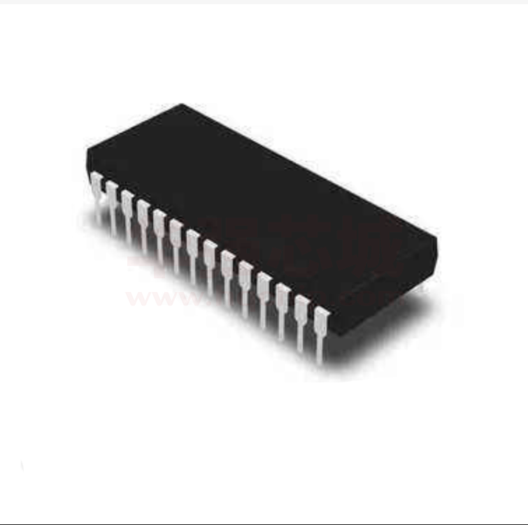
•28-pin Plastic DIP (DIP28-P-600-2.54)
PIN CONFIGURATION (TOP VIEW)
28 pin Plastic DIP
D2
1
28 D1
D3
2
27 D0
RXD
3
26 VCC
GND
4
25 RXC
D4
5
24 DTR
D5
6
23 RTS
D6
7
22 DSR
D7
8
21 RESET
TXC
9
20 CLK
WR 10
19 TXD
18 TXEMPTY
CS 11
C/D 12
17 CTS
RD 13
16 SYNDET/BD
15 TXRDY
RXRDY 14
http://www.hgsemi.com.cn
1
2018 AUG
�HG82C51
D7 - D0
Data Bus
Buffer
RESET
CLK
C/D
RD
WR
CS
Read/Write
Control
Logic
DSR
DTR
CTS
RTS
http://www.hgsemi.com.cn
Modem
Control
Internal Bus Line
FUNCTIONAL BLOCK DIAGRAM
2
Transmit
Buffer
(P - S)
TXD
Transmit
Control
TXRDY
TXE
TXC
Recieve
Buffer
(S - P)
RXD
Recieve
Control
RXRDY
RXC
SYNDET/BD
2018 AUG
�HG82C51
FUNCTION
Outline
The HG82C51's functional configuration is programed by software.
Operation between the HG82C51 and a CPU is executed by program control. Table 1
shows the operation between a CPU and the device.
Table 1 Operation between HG82C51 and CPU
CS
C/D
RD
WR
1
¥
¥
¥
Data Bus 3-State
0
¥
1
1
Data Bus 3-State
0
1
0
1
Status Æ CPU
0
1
1
0
Control Word ¨ CPU
0
0
0
1
Data Æ CPU
0
0
1
0
Data ¨ CPU
It is necessary to execute a function-setting sequence after resetting the HG82C51. Fig. 1
shows the function-setting sequence.
If the function was set, the device is ready to receive a command, thus enabling the transfer of
data by setting a necessary command, reading a status and reading/writing data.
External Reset
Internal Reset
Write Mode Instruction
Asynchronous
yes
no
Write First Sync
Charactor
Single
Sync Mode
yes
no
Write Second Sync
Charactor
End of Mode Setting
Fig. 1 Function-setting Sequence (Mode Instruction Sequence)
http://www.hgsemi.com.cn
3
2018 AUG
�HG82C51
Control Words
There are two types of control word.
1. Mode instruction (setting of function)
2. Command (setting of operation)
1) Mode Instruction
Mode instruction is used for setting the function of the HG82C51. Mode instruction
will be in “wait for write” at either internal reset or external reset. That is, the writing of a
control word after resetting will be recognized as a “mode instruction.”
Items set by mode instruction are as follows:
•
•
•
•
•
•
•
Synchronous/asynchronous mode
Stop bit length (asynchronous mode)
Character length
Parity bit
Baud rate factor (asynchronous mode)
Internal/external synchronization (synchronous mode)
Number of synchronous characters (Synchronous mode)
The bit configuration of mode instruction is shown in Figures 2 and 3. In the case of
synchronous mode, it is necessary to write one-or two byte sync characters.
If sync characters were written, a function will be set because the writing of sync characters
constitutes part of mode instruction.
D7
D6
D5
D4
D3
D2
D1
D0
S1
S1
EP
PEN
L2
L1
B2
B1
Baud Rate Factor
0
1
0
1
0
Refer to
Fig. 3
SYNC
0
1
1
1 ¥
16 ¥
64 ¥
Charactor Length
0
1
0
1
0
0
1
1
5 bits
6 bits
7 bits
8 bits
Parity Check
0
1
0
1
0
0
Odd
Parity
1
1
Even
Parity
Disable
Disable
Stop bit Length
0
1
0
0
0
1
1
1
Inhabit
1 bit
1.5 bits
2 bits
Fig. 2 Bit Configuration of Mode Instruction (Asynchronous)
http://www.hgsemi.com.cn
4
2018 AUG
�HG82C51
D7
D6
D5
D4
D3
D2
D1
D0
SCS
ESD
EP
PEN
L2
L1
0
0
Charactor Length
0
1
0
1
0
0
1
1
5 bits
6 bits
7 bits
8 bits
0
1
0
1
0
0
Odd
Parity
1
1
Even
Parity
Parity
Disable
Disable
Synchronous Mode
0
1
Internal
Synchronization
External
Synchronization
Number of Synchronous Charactors
0
1
2 Charactors
1 Charactor
Fig. 3 Bit Configuration of Mode Instruction (Synchronous)
http://www.hgsemi.com.cn
5
2018 AUG
�HG82C51
2) Command
Command is used for setting the operation of the HG82C51.
It is possible to write a command whenever necessary after writing a mode instruction and
sync characters.
Items to be set by command are as follows:
• Transmit
Enable/Disable
• Receive Enable/Disable
• DTR, RTS
Output of data.
• Resetting of error flag.
• Sending to break characters
• Internal resetting
• Hunt mode (synchronous mode)
The bit configuration of a command is shown in Fig. 4.
D7
D6
D5
D4
D3
D2
D1
D0
EH
IR
RTS
ER
SBRK
RXE
DTR
TXEN
1ºTransmit Enable
0ºDisable
DTR
1 Æ DTR = 0
0 Æ DTR = 1
1ºRecieve Enable
0ºDisable
1ºSent Break Charactor
0ºNormal Operation
1ºReset Error Flag
0ºNormal Operation
RTS
1 Æ RTS = 0
0 Æ RTS = 1
1ºInternal Reset
0ºNormal Operation
1ºHunt Mode (Note)
0ºNormal Operation
Note: Seach mode for synchronous
charactors in synchronous mode.
Fig. 4 Bit Configuration of Command
http://www.hgsemi.com.cn
6
2018 AUG
�HG82C51
Status Word
It is possible to see the internal status of HG82C51 by reading a status word.
The bit configuration of status word is shown in Fig. 5.
D7
D6
D5
D4
D3
D2
D1
D0
DSR
SYNDET
/BD
FE
OE
PE
TXEMPTY
RXRDY
TXRDY
Parity Different from
TXRDY Terminal.
Refer to "Explanation"
of TXRDY Terminals.
Same as terminal.
Refer to "Explanation"
of Terminals.
1ºParity Error
1ºOverrun Error
1ºFraming Error
Note: Only asynchronous mode.
Stop bit cannot be detected.
Shows Terminal DSR
1ºDSR = 0
0ºDSR = 1
Fig. 5 Bit Configuration of Status Word
Standby Status
It is possible to put the HG82C51 in Ústandby statusÛ
When the following conditions have been satisfied the HG82C51 is in Ústandby status.Û
(1) CS terminal is fixed at Vcc level.
(2) Input pins other CS , D0 to D7, RD, WR and C/D are fixed at Vcc or GND level (including
SYNDET in external synchronous mode).
Note:
When all output currents are 0, ICCS specification is applied.
http://www.hgsemi.com.cn
7
2018 AUG
�HG82C51
Pin Description
D0 to D7 (l/O terminal)
This is bidirectional data bus which receive control words and transmits data from the CPU and
sends status words and received data to CPU.
RESET (Input terminal)
A ÚHighÛ on this input forces the HG82C51 into Úreset status.Û
The device waits for the writing of “mode instruction.”
The min. reset width is six clock inputs during the operating status of CLK.
CLK (Input terminal)
CLK signal is used to generate internal device timing.
CLK signal is independent of RXC or TXC.
However, the frequency of CLK must be greater than 30 times the RXC and TXC at Synchronous
mode and Asynchronous “x1” mode, and must be greater than 5 times at Asynchronous “x16”
and “x64” mode.
WR (Input terminal)
This is the “active low” input terminal which receives a signal for writing transmit data and
control words from the CPU into the HG82C51.
RD (Input terminal)
This is the “active low” input terminal which receives a signal for reading receive data and
status words from the HG82C51.
C/D (Input terminal)
This is an input terminal which receives a signal for selecting data or command words and status
words when the HG82C51 is accessed by the CPU.
If C/D = low, data will be accessed.
If C/D = high, command word or status word will be accessed.
CS (Input terminal)
This is the Úactive lowÛ input terminal which selects the HG82C51 at low level when the
CPU accesses.
Note: The device won’t be in “standby status”; only setting CS = High.
Refer to “Explanation of Standby Status.”
TXD (output terminal)
This is an output terminal for transmitting data from which serial-converted data is sent out.
The device is in “mark status” (high level) after resetting or during a status when transmit is
disabled. It is also possible to set the device in “break status” (low level) by a command.
http://www.hgsemi.com.cn
8
2018 AUG
�HG82C51
TXRDY (output terminal)
This is an output terminal which indicates that the HG82C51 is ready to accept a
transmitted data character. But the terminal is always at low level if CTS = high or the device
was set in “TX disable status” by a command.
Note: TXRDY status word indicates that transmit data character is receivable,
regardless
of CTS or command.
If the CPU writes a data character, TXRDY will be reset by the leading edge or WR
signal.
TXEMPTY (Output terminal)
This is an output terminal which indicates that the HG82C51 has transmitted all the
characters and had no data character.
In “synchronous mode,” the terminal is at high level, if transmit data characters are no longer
remaining and sync characters are automatically transmitted. If the CPU writes a data
character, TXEMPTY will be reset by the leading edge of WR signal.
Note : As the transmitter is disabled by setting CTS “High” or command, data written
before disable will be sent out. Then TXD and TXEMPTY will be “High”.
Even if a data is written after disable, that data is not sent out and TXE will be
“High”.After
the transmitter is enabled, it sent out. (Refer to Timing Chart of
Transmitter Control and Flag
Timing)
TXC (Input terminal)
This is a clock input signal which determines the transfer speed of transmitted data.
In “synchronous mode,” the baud rate will be the same as the frequency of TXC.
In “asynchronous mode”, it is possible to select the baud rate factor by mode instruction.
It can be 1, 1/16 or 1/64 the TXC.
The falling edge of TXC sifts the serial data out of the HG82C51.
RXD (input terminal)
This is a terminal which receives serial data.
RXRDY (Output terminal)
This is a terminal which indicates that the HG82C51 contains a character that is ready to
READ.
If the CPU reads a data character, RXRDY will be reset by the leading edge of RD signal.
Unless the CPU reads a data character before the next one is received completely, the preceding
data will be lost. In such a case, an overrun error flag status word will be set.
RXC (Input terminal)
This is a clock input signal which determines the transfer speed of received data.
In “synchronous mode,” the baud rate is the same as the frequency of RXC.
In “asynchronous mode,” it is possible to select the baud rate factor by mode instruction.
It can be 1, 1/16, 1/64 the RXC.
http://www.hgsemi.com.cn
9
2018 AUG
�HG82C51
SYNDET/BD (Input or output terminal)
This is a terminal whose function changes according to mode.
In “internal synchronous mode.” this terminal is at high level, if sync characters are received and
synchronized. If a status word is read, the terminal will be reset.
In “external synchronous mode, “this is an input terminal.
A ÚHighÛ on this input forces the HG82C51 to start receiving data characters.
In “asynchronous mode,” this is an output terminal which generates “high level”output upon
the detection of a “break” character if receiver data contains a “low-level” space between the
stop bits of two continuous characters. The terminal will be reset, if RXD is at high level.
After Reset is active, the terminal will be output at low level.
DSR (Input terminal)
This is an input port for MODEM interface. The input status of the terminal can be recognized
by the CPU reading status words.
DTR (Output terminal)
This is an output port for MODEM interface. It is possible to set the status of DTR by a command.
CTS (Input terminal)
This is an input terminal for MODEM interface which is used for controlling a transmit circuit.
The terminal controls data transmission if the device is set in “TX Enable” status by a command.
Data is transmitable if the terminal is at low level.
RTS (Output terminal)
This is an output port for MODEM interface. It is possible to set the status RTS by a command.
http://www.hgsemi.com.cn
10
2018 AUG
�HG82C51
ABSOLUTE MAXIMUM RATING
Parameter
Symbol
Rating
Unit
Power Supply Voltage
VCC
–0.5 to +7
V
Input Voltage
VIN
–0.5 to VCC +0.5
V
VOUT
TSTG
–0.5 to VCC +0.5
V
–55 to +150
°C
—
W
Ta = 25°C
Output Voltage
Storage Temperature
Power Dissipation
0.9
PD
Conditions
With respect
to GND
OPERATING RANGE
Symbol
Range
Unit
Power Supply Voltage
Parameter
VCC
3-6
V
Operating Temperature
Top
°C
–40 to 85
RECOMMENDED OPERATING CONDITIONS
Parameter
Symbol
Min.
Typ.
Max.
Unit
Power Supply Voltage
VCC
4.5
5
5.5
V
Operating Temperature
Top
–40
+25
+85
°C
"L" Input Voltage
VIL
–0.3
—
+0.8
V
"H" Input Voltage
VIH
2.2
—
VCC +0.3
V
DC CHARACTERISTICS
(VCC = 4.5 to 5.5 V Ta = –40°C to +85°C)
Parameter
Symbol
Min.
—
Typ.
—
Max.
0.45
VOH
3.7
—
ILI
–10
—
Output Leak Current
ILO
–10
Operating Supply
Current
ICCO
Standby Supply
Current
ICCS
"L" Output Voltage
VOL
"H" Output Voltage
Input Leak Current
http://www.hgsemi.com.cn
Unit
Measurement Conditions
V
IOL = 2.5 mA
—
V
IOH = –2.5 mA
10
mA
0 £ VIN £ VCC
—
10
mA
0 £ VOUT £ VCC
—
—
5
mA
Asynchronous X64 during Transmitting/
Receiving
—
—
100
mA
All Input voltage shall be fixed at VCC or
GND level.
11
2018 AUG
�HG82C51
AC CHARACTERISTICS
CPU Bus Interface Part
(VCC = 4.5 to 5.5 V, Ta = –40 to 85°C)
Parameter
Address Stable before RD
Symbol
tAR
Min.
20
Max.
—
Unit
ns
Remarks
Note 2
Address Hold Time for RD
tRA
20
—
ns
Note 2
RD Pulse Width
tRR
130
—
ns
—
Data Delay from RD
tRD
—
100
ns
—
RD to Data Float
tDF
10
75
ns
Recovery Time between RD
tRVR
6
—
tCY
—
Note 5
Address Stable before WR
tAW
20
—
ns
Note 2
Address Hold Time for WR
tWA
20
—
ns
Note 2
WR Pulse Width
tWW
100
—
ns
Data Set-up Time for WR
tDW
100
—
ns
—
—
Data Hold Time for WR
tWD
0
—
ns
—
Recovery Time between WR
tRVW
6
—
tCY
Note 4
RESET Pulse Width
tRESW
6
—
tCY
—
http://www.hgsemi.com.cn
12
2018 AUG
�HG82C51
Serial Interface Part
(VCC = 4.5 to 5.5 V, Ta = –40 to 85°C)
Parameter
Symbol
Max.
—
Unit
Remarks
Main Clock Period
tCY
Min.
160
ns
Note 3
Clock Low Tme
tf
50
—
ns
—
Clock High Time
tf
70
tCY –50
ns
—
Clock Rise/Fall Time
tr, tf
—
20
ns
—
TXD Delay from Falling Edge of TXC
tDTX
—
1
mS
—
fTX
DC
64
kHz
16 ¥ Baud
fTX
DC
615
kHz
64 ¥ Baud
fTX
DC
615
kHz
1 ¥ Baud
tTPW
13
—
tCY
16 ¥, 64 ¥ Baud
tTPW
2
—
tCY
—
—
1 ¥ Baud
tTPD
15
—
tCY
—
—
1 ¥ Baud
Transmitter Clock Frequency
Transmitter Clock Low Time
Transmitter Clock High Time
Receiver Clock Frequency
Receiver Clock Low Time
Receiver Clock High Time
Note 3
16 ¥, 64 ¥ Baud
tTPD
3
—
tCY
1 ¥ Baud
fRX
DC
64
kHz
16 ¥ Baud
fRX
DC
615
kHz
64 ¥ Baud
fRX
DC
615
kHz
1 ¥ Baud
tRPW
13
—
tCY
—
16 ¥, 64 ¥ Baud
tRPW
2
—
tCY
1 ¥ Baud
tRPD
15
—
tCY
16 ¥, 64 ¥ Baud
tRPD
3
—
tCY
—
—
—
tTXRDY
—
8
tCY
—
tTXRDY CLEAR
—
400
ns
—
tRXRDY
—
26
tCY
—
tRXRDY CLEAR
—
400
ns
—
tIS
—
26
tCY
—
Time from the Center of Last Bit to the Rise of
TXRDY
Time from the Leading Edge of WR to the Fall
of TXRDY
Time From the Center of Last Bit to the Rise of RXRDY
Time from the Leading Edge of RD to the Fall
of RXRDY
Internal SYNDET Delay Time from Rising Edge of RXC
SYNDET Setup Time for RXC
Note 3
tES
18
—
tCY
—
tTXEMPTY
20
—
tCY
—
tWC
8
—
tCY
—
tCR
20
—
tCY
—
RXD Setup Time for Rising Edge of RXC (1X Baud)
tRXDS
11
—
tCY
—
RXD Hold Time for Falling Edge of RXC (1X Baud)
tRXDH
17
—
tCY
—
TXE Delay Time from the Center of Last Bit
MODEM Control Signal Delay Time from Rising Edge
of WR
MODEM Control Signal Setup Time for Falling Edge
of RD
Notes: 1. AC characteristics are measured at 150 pF capacity load as an output load based on 0.8 V at
low level and 2.2 V at high level for output and 1.5 V for input.
2. Addresses are CS and C/D.
3. fTX or fRX £ 1/(30 Tcy) 1¥ Baud
fTX or fRX £ 1/(5 Tcy)
16¥, 64¥ Baud
4. This recovery time is mode Initialization only. Recovery time between command writes for
Asynchronous Mode is 8 tCY and for Synchronous Mode is 18 tCY.
Write Data is allowed only when TXRDY = 1.
5. This recovery time is Status read only.
Read Data is allowed only when RXRDY = 1.
6. Status update can have a maximum delay of 28 clock periods from event affecting the status.
http://www.hgsemi.com.cn
13
2018 AUG
�HG82C51
TIMING CHART
Sytem Clock Input
tf
tr
tf
tf
tCY
CLK
Transmitter Clock and Data
tTPW
TXC (1 ¥ MODE)
tTPD
TXC (16 ¥ MODE)
tDTX
tDTX
TXD
Receiver Clock and Data
RXD
RXC (1 ¥ Mode)
RXC (16 ¥ Mode)
(RXBAUD Counter starts here)
Start bit
tRPW
8RXC Periods
(16¥Mode)
http://www.hgsemi.com.cn
Data bit
16 RXC Periods (16 ¥ Mode)
3tCY
INT Sampling
Pulse
Data bit
tRPD
3tCY
tf
14
2018 AUG
�HG82C51
Write Data Cycle (CPU Æ USART)
TXRDY
tWW
WR
DATA IN (D. B.)
tTXRDY Clear
tWD
tDW
Don't Care
Don't Care
Data Stable
C/D
tAW
tWA
CS
tAW
tWA
Read Data Cycle (CPU ¨ USART)
RXRDY
tRXRDY Clear
tRR
RD
DATA OUT (D. B.)
tRD
Data Float
tDF
Data Float
Data Out Active
C/D
tAR
tRA
CS
tAR
tRA
Write Control or Output Port Cycle (CPU Æ USART)
DTR. RTS
DATA IN
(D. B.)
tWC
tWW
WR
tWD
tDW
Don't Care
Don't Care
Data Stable
C/D
CS
tAW
tWA
tAW
tWA
Read Control or Input Port Cycle (CPU ¨ USART)
DSR. CTS
tCR
tRR
RD
DATA OUT
(D. B.)
tDF
Data Float
tRD
Data Out Active
Data Float
tAR
tRA
tAR
tRA
C/D
CS
http://www.hgsemi.com.cn
15
2018 AUG
�HG82C51
Transmitter Control and Flag Timing (ASYNC Mode)
CTS
tTXEMPTY
TXEMPTY
TXRDY
(STATUS BIT)
tTXRDY
TXRDY
(PIN)
Wr DATA 1
Wr DATA 2
Wr DATA 3
Wr DATA 4
C/D
Wr TxEn
Wr SBRK
WR
0
1
2
3
4
5
6
TXD
DATA CHAR 2
DATA CHAR 3
DATA CHAR 4
STOP BIT
START BIT
DATA CHAR 1
Note: The wave-form chart is based on the case of 7-bit data length + parity bit + 2 stop bit.
Receiver Control and Flag Timing (ASYNC Mode)
BREAK DETECT
FRAMING ERROR
(Status Bit)
OVERRUN ERROR
(Status Bit)
RXRDY
DATA
CHAR2
Lost
tRXRDY
Rd Data
C/D
WR
Wr RxEn
Wr Error
RxEn
RD
RXDATA
Data CHAR 2
Data CHAR 3
Break
RxEn Err Res
Data Bit
Start Bit
Stop Bit
Parity Bit
Data CHAR 1
Note: The wave-form chart is based on the case of 7 data bit length + parity bit + 2 stop bit.
Transmitter Control and Flag Timing (SYNC Mode)
CTS
TXEMPTY
TXRDY
(StatusBit)
TXRDY (Pin)
C/D
Wr Data
CHAR1
WR
Marking State
TXD
Wr Data
CHAR2
Wr Data
CHAR3
Wr Data
CHAR4
Wr Commond
SBRK
Data
Data
SYNC
SYNC
Data
Marking
CHAR1
CHAR2
CHAR1 SYNC CHAR2
CHAR3
CHAR4
State
0123 4 012 34 0 12 34 01234 012 34 0 123 4
PAR
PAR
PAR
PAR
PAR
PAR
Spacing
State
Wr Data
CHAR5
Marking
State
Data
SYNC
CHAR5
CHAR ETC
0123 4 012 34 0 1
PAR
PAR
Note: The wave-form chart is based on the case of 5 data bit length + parity bit and 2 synchronous charactors.
http://www.hgsemi.com.cn
16
2018 AUG
�HG82C51
Receiver Control and Flag Timing (SYNC Mode)
(Note 2)
SYNDET
(Pin) (Note 1)
tES
tIS
SYNDET (SB)
OVERRUN
ERROR (SB)
Data
CHAR2
Lost
RXRDY (PIN)
Rd Status
C/D
Wr EH
RxEn
Wr Err Res
Rd Data
CHAR 1
Rd Data
CHAR 3
Rd Status
Rd Status
Wr EHo
Rd SYNC
CHAR 1
WR
RD
Don't
Care
RXD
SYNC
CHAR 1
SYNC
CHAR 2
Data
CHAR 1
Data
CHAR 2
Data
CHAR 3
SYNC
CHAR 1
SYNC
CHAR 2 Don't Care
Data
CHAR 1
x x x x x x 0 1 2 3 4
0 1 2 3 4
0 1 2 3 4
0 1 2 3 4
0 1 2 3 4
0 1 2 3 4
0 1 2 3 4
0 1 2 3 4
PAR
PAR
PAR
PAR
CHAR ASSY Begins
RXC
PAR
Exit Hunt Mode
Set SYNDET
PAR
x x x x x x x
PAR
PAR
Data
CHAR 2
CHAR ASSY
Begins
Exit Hunt Mode
Set SYNDET (Status bit)
ETC
0 1 x 3 4
PAR
PAR
Set SYNDET (Status bit)
Note: 1. Internal Synchronization is based on the case of 5 data bit length + parity bit and 2 synchronous charactor.
2. External Synchronization is based on the case of 5 data bit length + parity bit.
Note: 1. Half-bit processing for the start bit
When the HG82C51 is used in the asynchronous mode, some problems are
caused in the processing for the start bit whose length is smaller than the 1-data bit
length. (See Fig. 1.)
Start bit Length
Mode
Operation
Smaller than 7-Receiver Clock Length
¥16
The short start bit is ignored. (Normal)
Smaller than 31-Receiver Clock Length
¥64
The short start bit is ignored. (Normal)
8-Receiver Clock Length
¥16
Data cannot be received correctly due to a malfunction.
32-Receiver Clock Length
¥64
Data cannot be received correctly due to a malfunction.
9 to 16-Receiver Clock Length
¥16
The bit is regarded as a start bit. (normal)
33 to 64-Receiver Clock Length
¥64
The bit is regarded as a start bit. (normal)
2. Parity flag after a break signal is received (See Fig. 2.)
When theHG82C51 is used in the asynchrous mode, a parity flag may be set
when the next normal data is read after a break signal is received.
A parity flag is set when the rising edge of the break signal (end of the break signal)
is changed between the final data bit and the parity bit, through a RXRDY signal may
not be outputted.
If this occurs, the parity flag is left set when the next normal dats is received, and the
received data seems to be a parity error.
http://www.hgsemi.com.cn
17
2018 AUG
�HG82C51
Half-bit Processing Timing Chart for the Start bit (Fig. 1)
Normal Operation
RXD
ST D0 D1 D2 D3 D4 D5 D6 D7 P SP
ST D0 D1 D2 D3 D4 D5 D6 D7 P SP
RXRDY
The Start bit Is Shorter Than a 1/2 Data bit
ST D0 D1 D2 D3 D4 D5 D6 D7 P SP
RXD
ST
RXRDY
The Start bit Is a 1/2 Data bit (A problem of HG82C51)
ST D0 D1 D2 D3 D4 D5 D6 D7 P SP
RXD
ST
RXRDY
A RXRDY signal is outputted during data
reception due to a malfunction.
The Start bit Is Longer Than a 1/2 Data bit
ST D0 D1 D2 D3 D4 D5 D6 D7 P SP
RXD
ST
RXRDY
ST:
SP:
P:
D0 - D7:
Start bit
Stop bit
Parity bit
Data bits
http://www.hgsemi.com.cn
18
2018 AUG
�HG82C51
Break Signal Reception Timing and Parity Flag (Fig. 2)
Normal Operation
BIT POS.
ST D0
D7 P SP ST D0
D7 P SP ST D0 D1 D2 D3 D4 D5 D6 D7 P SP
RXD
RXRDY
≠
No parity flag is set. and no RXRDY signal
is outputted.
Bug Timing
BIT POS.
ST D0
D7 P SP ST D0
D7 P SP ST D0 D1 D2 D3 D4 D5 D6 D7 P SP
RXD
RXRDY
≠
A parity flag is set, but, no RXRDYsignal
is outputted.
Normal Operation
BIT POS.
ST D0
D7 P SP ST D0
D7 P SP ST D0 D1 D2 D3 D4 D5 D6 D7 P SP
RXD
RXRDY
≠
A parity flag is set. and a RXRDY signal
is outputted.
http://www.hgsemi.com.cn
19
2018 AUG
�HG82C51
Important statement:
Huaguan Semiconductor Co,Ltd. reserves the right to change
the products and services provided without notice. Customers
should obtain the latest relevant information before ordering,
and verify the timeliness and accuracy of this information.
Customers are responsible for complying with safety
standards and taking safety measures when using our
products for system design and machine manufacturing to
avoid potential risks that may result in personal injury or
property damage.
Our products are not licensed for applications in life support,
military, aerospace, etc., so we do not bear the consequences
of the application of these products in these fields.
Our documentation is only permitted to be copied without
any tampering with the content, so we do not accept any
responsibility or liability for the altered documents.
http://www.hgsemi.com.cn
20
2018 AUG
�