HG9910
UNIVERSAL HIGH BRIGHTNESS LED DRIVER
FEATURES
Efficiency
Input voltage range
Withstanding input voltage surge
Output current range
String of LEDs
Constant-current LED driver
Linear and PWM dimming capability
PIN CONFIGURATION
>90%
10V to 600V
up to 600V
a few mA to more than 1A
1 pc to several hundreds
APPLICATIONS
DC/DC or AC/DC LED driver
RGB backlighting LED driver
Backlighting of flat panel displays
General-purpose constant current source
Signage and decorative LED lighting
Automotive
Chargers
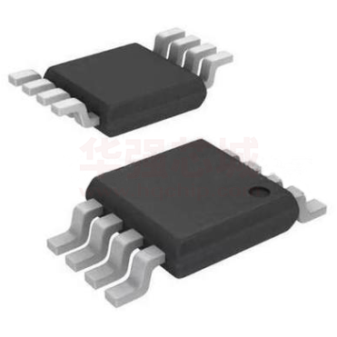
8-pin SO-8/DIP
VIN
1
8
Rosc
CS
2
7
CS
GND 3
6
VDD
Gate 4
5
PWM-D
DESCRIPTION
The HG9910 is a PWM high-efficiency LED driver control IC. It allows efficient operation of highbrightness (HB) LEDs from 10VDC up to 600VDC voltage sources. The circuit controls an external
MOSFET at fixed switching frequencies up to 300 kHz. The frequency can be programmed by using a
single resistor. The device peculiarity is that a LED string is driven at a constant current rather than at a
constant voltage, thus providing a constant light output and an enhanced reliability. The output current can
be programmed between a few milliamps and up to more than 1.0A. A rugged high-voltage junction
isolated process was used and enabled the device to withstand an input voltage surge up to 600V. The
output current to a LED string is programmable to any value between zero and its maximum value by
applying an external control voltage to the linear dimming control input. To allow the device to accept an
external control signal with a duty ratio of 0 to 100% and a frequency of up to a few kilohertz the circuit has
a low-frequency PWM dimming input.
TYPICAL APPLICATION CIRCUIT
CIN
VIN
VDD
HG9910
CDD
http://www.hgsemi.com.cn
1
2018 AUG
�HG9910
ABSOLUTE MAXIMUM RATINGS
VIN to GND
CS, LD, PWM_D, GATE to GND
Continuous power dissipation (TA = +25°C) (Note 1)
8-pin DIP (derate 9 mW/°C above +25°C)
8-pin SO-8 (derate 6.3 mW/°C above +25°C)
Operating temperature range
Junction temperature
Storage temperature range
-0.5V to +600V
-0.3V to VDD+0.3V
900mW
630mW
-40°C to +85°C
+125°C
-65°C to +150°C
Stresses beyond those listed under ABSOLUTE MAXIMUM RATINGS may cause permanent damage to the device. These are stress ratings only, and
functional operation of the device at these or any other conditions beyond those indicated in the operational sections of the specifications are not implied.
Exposure to absolute maximum rating conditions for extended periods may affect device reliability.
ELECTRICAL CHARACTERISTICS
(TA = +25°C unless noted otherwise)
DESCRIPTION
MIN
TYP
MAX
UNITS
CONDITIONS
VINDC
IINSD
VDD
SYMBOL
Input DC supply voltage range
Shut-down mode supply current
Internally regulated voltage
10.0
0.5
7.0
7.5
600
1
8.0
V
mA
V
ΔVDD, load
VDD load regulation
0
-
100
mV
DC input voltage
Pin PWM_D to GND, VIN = 8V
VIN = 10V to 600V, IDD(ext) = 0,
pin GATE is open
IDD(ext) = 0 to 1.0mA, 500pF at
GATE; ROSC = 226kOhm,
PWM_D = VDD
VDD,max
Maximal pin VDD voltage
10.0
V
IDD(ext)
VDD current available for external
circuitry
VDD undervoltage lockout
threshold
VDD undervoltage lockout
hysteresis
Pin PWM_D input low voltage
Pin PWM_D input high voltage
Pin PWM_D pull-down
resistance
Accuracy of Current Sense
threshold voltage at wafer
testing
Current sense pull-in threshold
voltage
GATE high output voltage
GATE low output voltage
Oscillator frequency
0.7
mA
0.91* VDD
%
Rising VIN
mV
Falling VIN
1
UVLO
ΔUVLO
VEN(lo)
VEN(hi)
REN
dVCS
VCS(hi)
VGATE(hi)
VGATE(lo)
fOSC
DMAX hf
TBLANK
tDELAY
Maximum oscillator PWM duty
cycle
Pin LD (linear dimming) voltage
range
Current sense blanking interval
Delay from CS to GATE lo
tRISE
tFALL
GATE output rise time
GATE output fall time
VLD
0.87* VDD
0.89* VDD
500
0.8
When an external voltage is
applied to pin VDD
VIN = 10V to 100V
2.0
50
100
150
V
V
kOhm
-2.4%
0
2.4%
%
238
250
262
mV
TA = -40°C to +85°C
VDD
0.3
30
120
100%
V
V
kHz
250
mV
IOUT = 10mA
IOUT = -10mA
ROSC = 1.00MOhm
ROSC = 226kOhm
FPWM hf = 25kHz, at GATE, CS
to GND
TA =
很抱歉,暂时无法提供与“HG9910M/TR”相匹配的价格&库存,您可以联系我们找货
免费人工找货- 国内价格
- 1+0.98005
- 30+0.94505
- 100+0.91005
- 500+0.84004
- 1000+0.80504
- 2000+0.78404