LM2576-XX
LM2576 Series
SIMPLE SWITCHER 3A Step-Down Voltage Regulator
General Description
Features
The LM2576 series of regulators are monolithic integrated
circuits that provide all the active functions for a step-down
(buck) switching regulator, capable of driving 3A load with
excellent line and load regulation. These devices are availableinfixedoutputvoltagesof3.3V,5V,12V,andan
adjustable output version.
Requiring a minimum number of external components, these
regulators are simple to use and include internal frequency
compensation and a fixed-frequency oscillator.
The LM2576 series offers a high-efficiency replacement for
popular three-terminal linear regulators. It substantially reduces the size of the heat sink, and in some cases no heat
sink is required.
A standard series of inductors optimized for use with the
LM2576 are available from several different manufacturers.
This feature greatly simplifies the design of switch-mode
power supplies.
Other features include a guaranteed ± 4% tolerance on output voltage within specified input voltages and output load
conditions, and ± 10% on the oscillator frequency. External
shutdown is included, featuring 50 µA (typical) standby current. The output switch includes cycle-by-cycle current limiting, as well as thermal shutdown for full protection under
fault conditions.
n 3.3V,5V,12V,andadjustableoutputversions
n Adjustable version output voltage range,
1.23Vto37V ± 4% max over
line and load conditions
n Guaranteed 3A output current
n Wideinputvoltagerange,40V
Typical Application
n
n
n
n
n
n
n
Requires only 4 external components
52 kHz fixed frequency internal oscillator
TTL shutdown capability, low power standby mode
High efficiency
Uses readily available standard inductors
Thermal shutdown and current limit protection
P+ Product Enhancement tested
Applications
n
n
n
n
Simple high-efficiency step-down (buck) regulator
Efficient pre-regulator for linear regulators
On-card switching regulators
Positive to negative converter (Buck-Boost)
(Fixed Output Voltage Versions)
FIGURE 1.
http://www.hgsemi.com.cn
1
2018 AUG
�LM2576-XX
Block Diagram
01147602
3.3V R2 = 1.7k
5V, R2 = 3.1k
For ADJ. Version
12V, R2 = 8.84k
R1 = Open, R2 = 0Ω
15V, R2 = 11.3k
Patent Pending
Absolute Maximum Ratings (Note 1)
Minimum ESD Rating
If Military/Aerospace specified devices are required,
please contact the National Semiconductor Sales Office/
Distributors for availability and specifications.
Lead Temperature
(C = 100 pF, R = 1.5 kΩ)
(Soldering, 10 Seconds)
2 kV
260˚C
Maximum Supply Voltage
LM2576
ON /OFF Pin Input Voltage
Operating Ratings
45V
Temperature Range
−0.3V ≤ V ≤ +VIN
LM2576
Output Voltage to Ground
(Steady State)
−1V
Power Dissipation
Internally Limited
Storage Temperature Range
−65˚C to +150˚C
Maximum Junction Temperature
http://www.hgsemi.com.cn
−40˚C ≤ TJ ≤ +125˚C
Supply Voltage
LM2576
40V
150˚C
2
2018 AUG
�LM2576-XX
LM2576-3.3
Electrical Characteristics
Specifications with standard type face are for TJ = 25˚C, and those with boldface type apply over full Operating Temperature
Range.
Symbol
Parameter
Conditions
LM2576-3.3
Typ
Limit
Units
(Limits)
(Note 2)
SYSTEM PARAMETERS (Note 3) Test Circuit Figure 2
VOUT
Output Voltage
VIN = 12V, ILOAD = 0.5A
3.3
V
Circuit of Figure 2
VOUT
η
Output Voltage
6V ≤ VIN ≤ 40V, 0.5A ≤ ILOAD ≤ 3A
LM2576
Circuit of Figure 2
Efficiency
3.234
V(Min)
3.366
V(Max)
3.168/3.135
V(Min)
3.432/3.465
V(Max)
3.3
VIN = 12V, ILOAD = 3A
V
75
%
LM2576-5.0
Electrical Characteristics
Specifications with standard type face are for TJ = 25˚C, and those with Figure 2 boldface type apply over full Operating Temperature Range.
Symbol
Parameter
Conditions
LM2576-5.0
Typ
Units
(Limits)
Limit
(Note 2)
SYSTEM PARAMETERS (Note 3) Test Circuit Figure 2
VOUT
Output Voltage
VIN = 12V, ILOAD = 0.5A
5.0
Circuit of Figure 2
VOUT
Output Voltage
LM2576
http://www.hgsemi.com.cn
0.5A ≤ ILOAD ≤ 3A,
V
4.900
V(Min)
5.100
V(Max)
5.0
V
8V ≤ VIN ≤ 40V
4.800/4.750
V(Min)
Circuit of Figure 2
5.200/5.250
V(Max)
3
2018 AUG
�LM2576-XX
LM2576-5.0
Electrical Characteristics
Specifications with standard type face are for TJ = 25˚C, and those with Figure 2 boldface type apply over full Operating Temperature Range.
Symbol
Parameter
Conditions
LM2576-5.0
Typ
Units
(Limits)
Limit
(Note 2)
SYSTEM PARAMETERS (Note 3) Test Circuit Figure 2
η
Efficiency
VIN = 12V, ILOAD = 3A
77
%
LM2576-12
Electrical Characteristics
Specifications with standard type face are for TJ = 25˚C, and those with boldface type apply over full Operating Temperature
Range.
Symbol
Parameter
Conditions
LM2576-12
Typ
Units
(Limits)
Limit
(Note 2)
SYSTEM PARAMETERS (Note 3) Test Circuit Figure 2
VOUT
Output Voltage
VIN = 25V, ILOAD = 0.5A
12
Circuit of Figure 2
VOUT
η
V
11.76
V(Min)
12.24
V(Max)
Output Voltage
0.5A ≤ ILOAD ≤ 3A,
LM2576
15V ≤ VIN ≤ 40V
11.52/11.40
V(Min)
Circuit of Figure 2
12.48/12.60
V(Max)
Efficiency
http://www.hgsemi.com.cn
VIN = 15V, ILOAD = 3A
4
12
88
V
%
2018 AUG
�LM2576-XX
Specifications with standard type face are for TJ = 25˚C, and those with boldface type apply over full Operating Temperature
Range.
Symbol
Parameter
Conditions
LM2576-ADJ
Typ
Units
(Limits)
Limit
(Note 2)
SYSTEM PARAMETERS (Note 3) Test Circuit Figure 2
VOUT
VOUT
η
Feedback Voltage
VIN = 12V, ILOAD = 0.5A
1.230
V
VOUT = 5V,
1.217
V(Min)
Circuit of Figure 2
1.243
V(Max)
Feedback Voltage
0.5A ≤ ILOAD ≤ 3A,
LM2576
8V ≤ VIN ≤ 40V
1.193/1.180
V(Min)
VOUT = 5V, Circuit of Figure 2
1.267/1.280
V(Max)
Efficiency
1.230
VIN = 12V, ILOAD = 3A, VOUT = 5V
V
77
%
All Output Voltage Versions Electrical Characteristics
Specifications with standard type face are for TJ = 25˚C, and those with boldface type apply over full Operating Temperature
Range. Unless otherwise specified, VIN = 12V for the 3.3V, 5V, and Adjustable version, VIN = 25V for the 12V version, and VIN
= 30V for the 15V version. ILOAD = 500 mA.
Symbol
Parameter
Conditions
LM2576-XX
Typ
Units
(Limits)
Limit
(Note 2)
DEVICE PARAMETERS
Ib
Feedback Bias Current
VOUT = 5V (Adjustable Version Only)
50
fO
Oscillator Frequency
(Note 11)
52
VSAT
Saturation Voltage
IOUT = 3A (Note 4)
Max Duty Cycle (ON)
(Note 5)
98
ICL
Current Limit
(Notes 4, 11)
5.8
Output Leakage Current
(Notes 6, 7):
Output = 0V
Output = −1V
IQ
Quiescent Current
(Note 6)
5
ISTBY
Standby Quiescent
ON /OFF Pin = 5V (OFF)
50
Current
http://www.hgsemi.com.cn
5
47/42
kHz
(Min)
58/63
kHz
(Max)
1.8/2.0
V(Max)
V
%
93
%(Min)
4.2/3.5
A(Min)
A
6.9/7.5
A(Max)
2
mA(Max)
30
mA(Max)
7.5
Output = −1V
nA
kHz
1.4
DC
IL
100/500
mA
mA
10
mA(Max)
200
µA(Max)
µA
2018 AUG
�LM2576-XX
Specifications with standard type face are for TJ = 25˚C, and those with boldface type apply over full Operating Temperature
Range. Unless otherwise specified, VIN = 12V for the 3.3V, 5V, and Adjustable version, VIN = 25V for the 12V version, and VIN
= 30V for the 15V version. ILOAD = 500 mA.
Symbol
Parameter
Conditions
LM2576-XX
Typ
Units
(Limits)
Limit
(Note 2)
DEVICE PARAMETERS
θJA
T Package, Junction to Ambient (Note 8)
65
θJA
Thermal Resistance
T Package, Junction to Ambient (Note 9)
45
θJC
T Package, Junction to Case
2
θJA
S Package, Junction to Ambient (Note 10)
50
˚C/W
ON /OFF CONTROL Test Circuit Figure 2
VIH
ON /OFF Pin
VOUT = 0V
1.4
2.2/2.4
V(Min)
VIL
Logic Input Level
VOUT = Nominal Output Voltage
1.2
1.0/0.8
V(Max)
IIH
ON /OFF Pin Input
ON /OFF Pin = 5V (OFF)
12
ON /OFF Pin = 0V (ON)
0
Current
IIL
µA
30
µA(Max)
10
µA(Max)
µA
Note 1: Absolute Maximum Ratings indicate limits beyond which damage to the device may occur. Operating Ratings indicate conditions for which the device is
intended to be functional, but do not guarantee specific performance limits. For guaranteed specifications and test conditions, see the Electrical Characteristics.
Note 2: All limits guaranteed at room temperature (standard type face) and at temperature extremes (bold type face). All room temperature limits are 100%
production tested. All limits at temperature extremes are guaranteed via correlation using standard Statistical Quality Control (SQC) methods.
Note 3: External components such as the catch diode, inductor, input and output capacitors can affect switching regulator system performance. When the
Figure 2 test circuit, system performance will be as shown in system parameters section of Electrical Characteristics.
LM2576 isusedasshowninthe
Note 4: Output pin sourcing current. No diode, inductor or capacitor connected to output.
Note 5: Feedback pin removed from output and connected to 0V.
Note 6: Feedback pin removed from output and connected to +12V for the Adjustable, 3.3V, and 5V versions, and +25V for the 12V and 15V versions, to force the
output transistor OFF.
Note 7: VIN = 40V (60V for high voltage version).
Note 8: Junction to ambient thermal resistance (no external heat sink) for the 5 lead TO-220 package mounted vertically, with 1⁄2 inch leads in a socket, or on a PC
board with minimum copper area.
Note 9: Junction to ambient thermal resistance (no external heat sink) for the 5 lead TO-220 package mounted vertically, with 1⁄4 inch leads soldered to a PC board
containing approximately 4 square inches of copper area surrounding the leads.
Note 10: If the TO-263 package is used, the thermal resistance can be reduced by increasing the PC board copper area thermally connected to the package. Using
0.5 square inches of copper area, θJA is 50˚C/W, with 1 square inch of copper area, θJA is 37˚C/W, and with 1.6 or more square inches of copper area, θJA is 32˚C/W.
Note 11: The oscillator frequency reduces to approximately 11 kHz in the event of an output short or an overload which causes the regulated output voltage to drop
approximately 40% from the nominal output voltage. This self protection feature lowers the average power dissipation of the IC by lowering the minimum duty cycle
from 5% down to approximately 2%.
Typical Performance Characteristics
(Circuit of Figure 2)
Normalized Output Voltage
http://www.hgsemi.com.cn
Line Regulation
6
2018 AUG
�LM2576-XX
Typical Performance Characteristics (Circuit of Figure 2)
Dropout Voltage
(Continued)
Current Limit
01147630
01147629
Standby
Quiescent Current
Quiescent Current
01147631
01147632
Switch Saturation
Voltage
Oscillator Frequency
01147634
01147633
http://www.hgsemi.com.cn
7
2018 AUG
�LM2576-XX
Typical Performance Characteristics (Circuit of Figure 2)
Efficiency
(Continued)
Minimum Operating Voltage
01147635
01147636
Quiescent Current
vs Duty Cycle
Feedback Voltage
vs Duty Cycle
01147637
01147638
Quiescent Current
vs Duty Cycle
Minimum Operating Voltage
01147636
http://www.hgsemi.com.cn
01147637
8
2018 AUG
�LM2576-XX
LM2576 Series Buck Regulator Design Procedure
(Continued)
INDUCTOR VALUE SELECTION GUIDES (For Continuous Mode Operation)
DS011476-9
FIGURE 3. LM2576(HV)-3.3
DS011476-11
FIGURE 5. LM2576(HV)-12
DS011476-10
FIGURE 4. LM2576(HV)-5.0
FIGURE 7. LM2576(HV)-ADJ
http://www.hgsemi.com.cn
9
2018 AUG
�LM2576-XX
Single-point grounding (as indicated) or ground plane construction should be used for best results. When using the
Adjustable version, physically locate the programming resistors near the regulator, to keep the sensitive feedback wiring
short.
Test Circuit and Layout Guidelines
As in any switching regulator, layout is very important. Rapidly switching currents associated with wiring inductance
generate voltage transients which can cause problems. For
minimal inductance and ground loops, the length of the leads
indicated by heavy lines should be kept as short as possible.
Fixed Output Voltage Versions
01147607
CIN — 100 µF, 75V, Aluminum Electrolytic
COUT — 1000 µF, 25V, Aluminum Electrolytic
D1 — Schottky, MBR360
L1 — 100 µH, Pulse Eng. PE-92108
R1 — 2k, 0.1%
R2 — 6.12k, 0.1%
Adjustable Output Voltage Version
01147608
where VREF = 1.23V, R1 between 1k and 5k.
FIGURE 2.
http://www.hgsemi.com.cn
10
2018 AUG
�LM2576-XX
LM2576 Series Buck Regulator Design Procedure
PROCEDURE (Adjustable Output Voltage Versions)
EXAMPLE (Adjustable Output Voltage Versions)
2. Inductor Selection (L1) A. Calculate E • T (V • µs)
2. Inductor Selection (L1) A. Calculate the inductor Volt
• microsecond constant, E • T (V • µs), from the
following formula:
B. E • T = 115 V • µs C. ILOAD(Max) = 3A D. Inductance
Region = H150 E. Inductor Value = 150 µH Choose from
AIE part #415-0936 Pulse Engineering part #PE-531115,
or Renco part #RL2445.
B. Use the E • T value from the previous formula and
match it with the E • T number on the vertical axis of the
Inductor Value Selection Guide shown in Figure 7. C. On
the horizontal axis, select the maximum load current. D.
Identify the inductance region intersected by the E • T
value and the maximum load current value, and note the
inductor code for that region. E. Identify the inductor value
from the inductor code, and select an appropriate inductor
from the table shown in Figure 9. Part numbers are listed
for three inductor manufacturers. The inductor chosen
must be rated for operation at the LM2576 switching frequency (52 kHz) and for a current rating of 1.15 x ILOAD.
For additional inductor information, see the inductor section in the application hints section of this data sheet.
3. Output Capacitor Selection (COUT)
3. Output Capacitor Selection (COUT) A. The value of
the output capacitor together with the inductor defines
the dominate pole-pair of the switching regulator loop.
For stable operation, the capacitor must satisfy the
following requirement:
However, for acceptable output ripple voltage select COUT
≥ 680 µF COUT = 680 µF electrolytic capacitor
The above formula yields capacitor values between 10 µF
and 2200 µF that will satisfy the loop requirements for
stable operation. But to achieve an acceptable output
ripple voltage, (approximately 1% of the output voltage)
and transient response, the output capacitor may need to
be several times larger than the above formula yields. B.
The capacitor’s voltage rating should be at last 1.5 times
greater than the output voltage. For a 10V regulator, a
rating of at least 15V or more is recommended. Higher
voltage electrolytic capacitors generally have lower ESR
numbers, and for this reason it may be necessary to select
a capacitor rate for a higher voltage than would normally be
needed.
4. Catch Diode Selection (D1) A. The catch-diode
current rating must be at least 1.2 times greater than the
maximum load current. Also, if the power supply design
must withstand a continuous output short, the diode
should have a current rating equal to the maximum
current limit of the LM2576. The most stressful condition
for this diode is an overload or shorted output. See diode
selection guide in Figure 8. B. The reverse voltage rating
of the diode should be at least 1.25 times the maximum
input voltage.
4. Catch Diode Selection (D1) A. For this example, a
3.3A current rating is adequate. B. Use a 30V 31DQ03
Schottky diode, or any of the suggested fast-recovery
diodes in Figure 8.
5. Input Capacitor (CIN) An aluminum or tantalum
electrolytic bypass capacitor located close to the
regulator is needed for stable operation.
5. Input Capacitor (CIN) A 100 µF aluminum electrolytic
capacitor located near the input and ground pins
provides sufficient bypassing.
To further simplify the buck regulator design procedure, National Semiconductor is making available computer design
software to be used with the SIMPLE SWITCHER line of
http://www.hgsemi.com.cn
switching regulators. Switchers Made Simple (Version 3.3)
is available on a (31⁄2") diskette for IBM compatible computers from a National Semiconductor sales office in your area.
11
2018 AUG
�LM2576-XX
Additional Applications
The switch currents in this buck-boost configuration are
higher than in the standard buck-mode design, thus lowering
the available output current. Also, the start-up input current
of the buck-boost converter is higher than the standard
buck-mode regulator, and this may overload an input power
source with a current limit less than 5A. Using a delayed
turn-on or an undervoltage lockout circuit (described in the
next section) would allow the input voltage to rise to a high
enough level before the switcher would be allowed to turn
on.
Because of the structural differences between the buck and
the buck-boost regulator topologies, the buck regulator design procedure section can not be used to to select the
inductor or the output capacitor. The recommended range of
inductor values for the buck-boost design is between 68 µH
and 220 µH, and the output capacitor values must be larger
than what is normally required for buck designs. Low input
voltages or high output currents require a large value output
capacitor (in the thousands of micro Farads).
The peak inductor current, which is the same as the peak
switch current, can be calculated from the following formula:
01147615
Typical Load Current
400 mA for VIN = −5.2V
750 mA for VIN = −7V
Note: Heat sink may be required.
FIGURE 11. Negative Boost
Because of the boosting function of this type of regulator, the
switch current is relatively high, especially at low input voltages. Output load current limitations are a result of the
maximum current rating of the switch. Also, boost regulators
can not provide current limiting load protection in the event of
a shorted load, so some other means (such as a fuse) may
be necessary.
Where fosc = 52 kHz. Under normal continuous inductor
current operating conditions, the minimum VIN represents
the worst case. Select an inductor that is rated for the peak
current anticipated.
UNDERVOLTAGE LOCKOUT
In some applications it is desirable to keep the regulator off
until the input voltage reaches a certain threshold. An undervoltage lockout circuit which accomplishes this task is
shown in Figure 12, while Figure 13 shows the same circuit
applied to a buck-boost configuration. These circuits keep
the regulator off until the input voltage reaches a predetermined level.
VTH ≈ VZ1 + 2VBE(Q1)
01147614
FIGURE 10. Inverting Buck-Boost Develops −12V
Also, the maximum voltage appearing across the regulator is
the absolute sum of the input and output voltage. For a −12V
output, the maximum input voltage for the LM2576 is +28V,
or +48V for the LM2576HV.
The Switchers Made Simple (version 3.0) design software
can be used to determine the feasibility of regulator designs
using different topologies, different input-output parameters,
different components, etc.
01147616
Note: Complete circuit not shown.
NEGATIVE BOOST REGULATOR
Another variation on the buck-boost topology is the negative
boost configuration. The circuit in Figure 11 accepts an input
voltage ranging from −5V to −12V and provides a regulated
−12V output. Input voltages greater than −12V will cause the
output to rise above −12V, but will not damage the regulator.
http://www.hgsemi.com.cn
FIGURE 12. Undervoltage Lockout for Buck Circuit
12
2018 AUG
�LM2576-XX
Additional Applications
ing. Increasing the RC time constant can provide longer
delay times. But excessively large RC time constants can
cause problems with input voltages that are high in 60 Hz or
120 Hz ripple, by coupling the ripple into the ON /OFF pin.
ADJUSTABLE OUTPUT, LOW-RIPPLE POWER SUPPLY
A 3A power supply that features an adjustable output voltage
is shown in Figure 15. An additional L-C filter that reduces
the output ripple by a factor of 10 or more is included in this
circuit.
01147617
Note: Complete circuit not shown (see Figure 10).
FIGURE 13. Undervoltage Lockout
for Buck-Boost Circuit
DELAYED STARTUP
The ON /OFF pin can be used to provide a delayed startup
feature as shown in Figure 14. With an input voltage of 20V
and for the part values shown, the circuit provides approximately 10 ms of delay time before the circuit begins switch-
Note: Complete circuit not shown.
FIGURE 14. Delayed Startup
FIGURE15.1.2Vto37V Adjustable3APowerSupplywithLowOutputRipple
Definition of Terms
BUCK REGULATOR
A switching regulator topology in which a higher voltage is
converted to a lower voltage. Also known as a step-down
switching regulator.
CATCH DIODE OR CURRENT STEERING DIODE
BUCK-BOOST REGULATOR
A switching regulator topology in which a positive voltage is
converted to a negative voltage without a transformer.
The diode which provides a return path for the load current
when the LM2576 switch is OFF.
EFFICIENCY (η)
The proportion of input power actually delivered to the load.
DUTY CYCLE (D)
Ratio of the output switch’s on-time to the oscillator period.
http://www.hgsemi.com.cn
13
2018 AUG
�LM2576-XX
Definition of Terms
CAPACITOR EQUIVALENT SERIES RESISTANCE (ESR)
The purely resistive component of a real capacitor’s impedance (see Figure 16). It causes power loss resulting in
capacitor heating, which directly affects the capacitor’s operating lifetime. When used as a switching regulator output
filter, higher ESR values result in higher output ripple voltages.
Connection Diagrams
Straight Leads
5-Lead TO-220 (T)
Top View
01147621
LM2576T-XX
01147620
NS Package Number T05A
FIGURE 16. Simple Model of a Real Capacitor
Most standard aluminum electrolytic capacitors in the
100 µF–1000 µF range have 0.5Ω to 0.1Ω ESR. Highergrade capacitors (“low-ESR”, “high-frequency”, or “lowinductance”) in the 100 µF–1000 µF range generally have
ESR of less than 0.15Ω.
TO-263 (S)
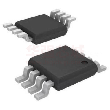
5-Lead Surface-Mount Package
Top View
EQUIVALENT SERIES INDUCTANCE (ESL)
The pure inductance component of a capacitor (see Figure
16). The amount of inductance is determined to a large
extent on the capacitor’s construction. In a buck regulator,
this unwanted inductance causes voltage spikes to appear
on the output.
OUTPUT RIPPLE VOLTAGE
The AC component of the switching regulator’s output voltage. It is usually dominated by the output capacitor’s ESR
multiplied by the inductor’s ripple current (∆IIND). The peakto-peak value of this sawtooth ripple current can be determined by reading the Inductor Ripple Current section of the
Application hints.
CAPACITOR RIPPLE CURRENT
RMS value of the maximum allowable alternating current at
which a capacitor can be operated continuously at a specified temperature.
01147625
LM2576S-XX
NS Package Number TS5B
LM2576SX-XX
NS Package Number TS5B, Tape and Reel
Bent, Staggered Leads
5-Lead TO-220 (T)
Top View
STANDBY QUIESCENT CURRENT (ISTBY)
Supply current required by the LM2576 when in the standby
mode (ON /OFF pin is driven to TTL-high voltage, thus
turning the output switch OFF).
INDUCTOR RIPPLE CURRENT (∆IIND)
The peak-to-peak value of the inductor current waveform,
typically a sawtooth waveform when the regulator is operating in the continuous mode (vs. discontinuous mode).
OPERATING VOLT MICROSECOND CONSTANT (E • Top)
The product (in VoIt • µs) of the voltage applied to the inductor
and the time the voltage is applied. This E • Top constant is a
measure of the energy handling capability of an inductor and
is dependent upon the type of core, the core area, the
number of turns, and the duty cycle.
http://www.hgsemi.com.cn
14
01147622
LM2576T-XX Flow LB03
NS Package Number T05D
2018 AUG
�