LM2596
LM2596
SIMPLE SWITCHER Power Converter 150 kHz
3A Step-Down Voltage Regulator
General Description
Features
The LM2596 series of regulators are monolithic integrated
circuits that provide all the active functions for a step-down
(buck) switching regulator, capable of driving a 3A load with
excellent line and load regulation. These devices are available in fixed output voltages of 3.3V, 5V, 12V, and an adjustable output version.
Requiring a minimum number of external components, these
regulators are simple to use and include internal frequency
compensation†, and a fixed-frequency oscillator.
The LM2596 series operates at a switching frequency of
150 kHz thus allowing smaller sized filter components than
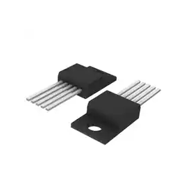
what would be needed with lower frequency switching regulators. Available in a standard 5-lead TO-220 package with
several different lead bend options, and a 5-lead TO-263
surface mount package.
A standard series of inductors are available from several
different manufacturers optimized for use with the LM2596
series. This feature greatly simplifies the design of
switch-mode power supplies.
Other features include a guaranteed ± 4% tolerance on output voltage under specified input voltage and output load
conditions, and ± 15% on the oscillator frequency. External
shutdown is included, featuring typically 80 µA standby current. Self protection features include a two stage frequency
reducing current limit for the output switch and an over
temperature shutdown for complete protection under fault
conditions.
n 3.3V, 5V, 12V, and adjustable output versions
n Adjustable version output voltage range, 1.2V to 37V
± 4% max over line and load conditions
n Available in TO-220 and TO-263 packages
n Guaranteed 3A output load current
n Input voltage range up to 40V
n Requires only 4 external components
n Excellent line and load regulation specifications
n 150 kHz fixed frequency internal oscillator
n TTL shutdown capability
n Low power standby mode, IQ typically 80 µA
n High efficiency
n Uses readily available standard inductors
n Thermal shutdown and current limit protection
Typical Application
Applications
n Simple high-efficiency step-down (buck) regulator
n On-card switching regulators
n Positive to negative converter
Note: †Patent Number 5,382,918.
(Fixed Output Voltage
Versions)
http://www.hgsemi.com.cn
1
2018 JUN
�LM2596
Connection Diagrams and Ordering Information
Bent and Staggered Leads, Through Hole
Package
5-Lead TO-220 (T)
Surface Mount Package
5-Lead TO-263 (S)
01258303
01258302
Order Number LM2596S-3.3, LM2596S-5.0,
LM2596S-12 or LM2596S-ADJ
See NS Package Number TS5B
Order Number LM2596T-3.3, LM2596T-5.0,
LM2596T-12 or LM2596T-ADJ
See NS Package Number T05D
Absolute Maximum Ratings
If Military/Aerospace specified devices are required,
please contact the National Semiconductor Sales Office/
Distributors for availability and specifications.
Maximum Supply Voltage
ON /OFF Pin Input Voltage
45V
−0.3 ≤ V ≤+25V
Power Dissipation
Internally limited
ESD Susceptibility HumanBodyModel
S Package
−0.3 ≤ V ≤ +25V
Feedback Pin Voltage
Output Voltage to Ground
(Steady State)
StorageTemperatureRange
Lead Temperature
−1V
−65˚Cto+150˚C
Vapor Phase (60 sec.)
+215˚C
Infrared (10 sec.)
+245˚C
T Package (Soldering, 10 sec.)
+260˚C
Maximum Junction Temperature
+150˚C
Operating Conditions
2kV
Temperature Range
Supply Voltage
http://www.hgsemi.com.cn
2
−40˚C ≤ TJ ≤ +125˚C
4.5V to 40V
2018 JUN
�LM2596
LM2596-3.3
Electrical Characteristics
Specifications with standard type face are for TJ = 25˚C, and those with boldface type apply over full Operating Temperature Range
LM2596-3.3
Symbol
Parameter
Conditions
Typ
(Note 3)
Limit
(Note 4)
Units
(Limits)
SYSTEM PARAMETERS (Note 5) Test Circuit Figure 1
VOUT
η
Output Voltage
Efficiency
4.75V ≤ VIN ≤ 40V, 0.2A ≤ ILOAD ≤ 3A
V IN = 12V, I LOAD = 3A
3.3
V
3.168/3.135
V(min)
3.432/3.465
V(max)
%
73
LM2596-5.0
Electrical Characteristics
Specifications with standard type face are for TJ = 25˚C, and those with boldface type apply over full Operating Temperature Range
LM2596-5.0
Symbol
Parameter
Conditions
Typ
(Note 3)
Limit
(Note 4)
Units
(Limits)
SYSTEM PARAMETERS (Note 5) Test Circuit Figure 1
VOUT
η
Output Voltage
Efficiency
7V ≤ VIN ≤ 40V, 0.2A ≤ ILOAD ≤ 3A
VIN = 12V, ILOAD = 3A
5.0
V
4.800/4.750
V(min)
5.200/5.250
V(max)
80
%
LM2596-12
Electrical Characteristics
Specifications with standard type face are for TJ = 25˚C, and those with boldface type apply over full Operating Temperature Range
LM2596-12
Symbol
Parameter
Conditions
Typ
(Note 3)
Limit
(Note 4)
Units
(Limits)
SYSTEM PARAMETERS (Note 5) Test Circuit Figure 1
VOUT
η
Output Voltage
Efficiency
http://www.hgsemi.com.cn
15V ≤ VIN ≤ 40V, 0.2A ≤ ILOAD ≤ 3A
VIN = 25V, ILOAD = 3A
12.0
90
3
V
11.52/11.40
V(min)
12.48/12.60
V(max)
%
2018 JUN
�LM2596
Specifications with standard type face are for TJ = 25˚C, and those with boldface type apply over full Operating Temperature Range
LM2596-ADJ
Symbol
Parameter
Conditions
Typ
(Note 3)
Limit
(Note 4)
Units
(Limits)
SYSTEM PARAMETERS (Note 5) Test Circuit Figure 1
VFB
Feedback Voltage
4.5V ≤ VIN ≤ 40V, 0.2A ≤ ILOAD ≤ 3A
1.230
V
VOUT programmed for 3V. Circuit of Figure 1
η
Efficiency
VIN = 12V, VOUT = 3V, ILOAD = 3A
1.193/1.180
V(min)
1.267/1.280
V(max)
73
%
All Output Voltage Versions Electrical Characteristics
Specifications with standard type face are for TJ = 25˚C, and those with boldface type apply over full Operating Temperature Range. Unless otherwise specified, VIN = 12V for the 3.3V, 5V, and Adjustable version and VIN = 24V for the 12V version. ILOAD = 500 mA
LM2596-XX
Symbol
Parameter
Conditions
Typ
(Note 3)
Limit
(Note 4)
Units
(Limits)
DEVICE PARAMETERS
Ib
fO
VSAT
DC
ICL
IL
Feedback Bias Current
Oscillator Frequency
Saturation Voltage
Adjustable Version Only, VFB = 1.3V
(Note 6)
IOUT = 3A (Notes 7, 8)
Max Duty Cycle (ON)
(Note 8)
100
(Note 9)
0
Current Limit
Peak Current (Notes 7, 8)
Quiescent Current
nA (max)
127/110
kHz(min)
173/173
kHz(max)
1.4/1.5
V(max)
kHz
1.16
Min Duty Cycle (OFF)
Output Leakage Current
nA
50/100
150
V
%
4.5
Output = 0V (Notes 7, 9)
Output = −1V (Note 10)
IQ
10
A
3.6/3.4
A(min)
6.9/7.5
A(max)
50
µA(max)
30
mA(max)
10
mA(max)
2
(Note 9)
mA
5
mA
ISTBY
Standby Quiescent Current
ON/OFF pin = 5V (OFF)
θJC
Thermal Resistance
TO-220 or TO-263 Package, Junction to Case
2
˚C/W
θJA
TO-220 Package, Junction to Ambient (Note 11)
50
˚C/W
θJA
TO-263 Package, Junction to Ambient (Note 12)
50
˚C/W
θJA
TO-263 Package, Junction to Ambient (Note 13)
30
˚C/W
θJA
TO-263 Package, Junction to Ambient (Note 14)
20
˚C/W
(Note 10)
80
µA
200/250
µA(max)
ON/OFF CONTROL Test Circuit Figure 1
ON /OFF Pin Logic Input
VIH
Threshold Voltage
VIL
http://www.hgsemi.com.cn
1.3
V
Low (Regulator ON)
0.6
V(max)
High (Regulator OFF)
2.0
V(min)
4
2018 JUN
�LM2596
All Output Voltage Versions
Electrical Characteristics
(Continued)
Specifications with standard type face are for TJ = 25˚C, and those with boldface type apply over full Operating Temperature Range. Unless otherwise specified, VIN = 12V for the 3.3V, 5V, and Adjustable version and VIN = 24V for the 12V version. ILOAD = 500 mA
LM2596-XX
Symbol
IH
Parameter
ON /OFF Pin Input Current
IL
Conditions
VLOGIC = 2.5V (Regulator OFF)
VLOGIC = 0.5V (Regulator ON)
Typ
(Note 3)
Limit
(Note 4)
Units
(Limits)
5
µA
15
µA(max)
5
µA(max)
0.02
µA
Note 1: Absolute Maximum Ratings indicate limits beyond which damage to the device may occur. Operating Ratings indicate conditions for which the device is
intended to be functional, but do not guarantee specific performance limits. For guaranteed specifications and test conditions, see the Electrical Characteristics.
Note 2: The human body model is a 100 pF capacitor discharged through a 1.5k resistor into each pin.
Note 3: Typical numbers are at 25˚C and represent the most likely norm.
Note 4: All limits guaranteed at room temperature (standard type face) and at temperature extremes (bold type face). All room temperature limits are 100%
production tested. All limits at temperature extremes are guaranteed via correlation using standard Statistical Quality Control (SQC) methods. All limits are used to
calculate Average Outgoing Quality Level (AOQL).
Note 5: External components such as the catch diode, inductor, input and output capacitors, and voltage programming resistors can affect switching regulator
system performance. When the LM2596 is used as shown in the Figure 1 test circuit, system performance will be as shown in system parameters section of Electrical
Characteristics.
Note 6: The switching frequency is reduced when the second stage current limit is activated.
Note 7: No diode, inductor or capacitor connected to output pin.
Note 8: Feedback pin removed from output and connected to 0V to force the output transistor switch ON.
Note 9: Feedback pin removed from output and connected to 12V for the 3.3V, 5V, and the ADJ. version, and 15V for the 12V version, to force the output transistor
switch OFF.
Note 10: VIN = 40V.
Note 11: Junction to ambient thermal resistance (no external heat sink) for the TO-220 package mounted vertically, with the leads soldered to a printed circuit board
with (1 oz.) copper area of approximately 1 in2.
Note 12: Junction to ambient thermal resistance with the TO-263 package tab soldered to a single printed circuit board with 0.5 in2 of (1 oz.) copper area.
Note 13: Junction to ambient thermal resistance with the TO-263 package tab soldered to a single sided printed circuit board with 2.5 in2 of (1 oz.) copper area.
Note 14: Junction to ambient thermal resistance with the TO-263 package tab soldered to a double sided printed circuit board with 3 in2 of (1 oz.) copper area on
the LM2596S side of the board, and approximately 16 in2 of copper on the other side of the p-c board. See Application Information in this data sheet and the thermal
model in Switchers Made Simple™ version 4.3 software.
Typical Performance Characteristics
Normalized
Output Voltage
http://www.hgsemi.com.cn
(Circuit of Figure 1)
Line Regulation
5
Efficiency
2018 JUN
�LM2596
Typical Performance Characteristics
(Circuit of Figure 1) (Continued)
Switch Saturation
Voltage
Switch Current Limit
Dropout Voltage
Operating
Shutdown
Minimum Operating
Quiescent Current
Quiescent Current
Supply Voltage
ON /OFF Threshold
Voltage
ON /OFF Pin
Current (Sinking)
Switching Frequency
http://www.hgsemi.com.cn
6
2018 JUN
�LM2596
LM2596 SeriesBuckRegulatorDesignProcedure(FixedOutput)
Conditions
Inductor
(Continued)
Output Capacitor
Through Hole Electrolytic
Surface Mount Tantalum
Output
Load
Max Input
Inductance
Inductor
Panasonic
Nichicon
AVX TPS
Sprague
Voltage
Current
Voltage
(µH)
(#)
HFQ Series
PL Series
Series
595D Series
(V)
(A)
(V)
(µF/V)
(µF/V)
(µF/V)
(µF/V)
3.3
3
470/25
560/16
330/6.3
390/6.3
5
2
5
3
2
12
3
2
22 L41
7
22 L41
560/35
560/35
330/6.3
390/6.3
10
22 L41
680/35
680/35
330/6.3
390/6.3
40
33 L40
560/35
470/35
330/6.3
390/6.3
6
22 L33
470/25
470/35
330/6.3
390/6.3
10
33 L32
330/35
330/35
330/6.3
390/6.3
40
47 L39
330/35
270/50
220/10
330/10
8
22 L41
470/25
560/16
220/10
330/10
10
22 L41
560/25
560/25
220/10
330/10
15
33 L40
330/35
330/35
220/10
330/10
40
47 L39
330/35
270/35
220/10
330/10
9
22 L33
470/25
560/16
220/10
330/10
20
68 L38
180/35
180/35
100/10
270/10
40
68 L38
180/35
180/35
100/10
270/10
15
22 L41
470/25
470/25
100/16
180/16
18
33 L40
330/25
330/25
100/16
180/16
30
68 L44
180/25
180/25
100/16
120/20
40
68 L44
180/35
180/35
100/16
120/20
15
33 L32
330/25
330/25
100/16
180/16
20
68 L38
180/25
180/25
100/16
120/20
40
150 L42
82/25
82/25
68/20
68/25
FIGURE 2. LM2596 Fixed Voltage Quick Design Component Selection Table
LM2596 SeriesBuckRegulatorDesignProcedure(AdjustableOutput)
Output
Voltage
(V)
Through Hole Output Capacitor
Surface Mount Output Capacitor
Panasonic
Nichicon PL
Feedforward
AVX TPS
Sprague
Feedforward
HFQ Series
Series
Capacitor
Series
595D Series
Capacitor
(µF/V)
(µF/V)
(µF/V)
(µF/V)
2
820/35
820/35
33 nF
330/6.3
470/4
4
560/35
470/35
10 nF
330/6.3
390/6.3
10 nF
6
470/25
470/25
3.3 nF
220/10
330/10
3.3 nF
9
330/25
330/25
1.5 nF
100/16
180/16
1.5 nF
12
330/25
330/25
1 nF
100/16
180/16
1 nF
15
220/35
220/35
680 pF
68/20
120/20
680 pF
24
220/35
150/35
560 pF
33/25
33/25
220 pF
28
100/50
100/50
390 pF
10/35
15/50
220 pF
33 nF
FIGURE 3. Output Capacitor and Feedforward Capacitor Selection Table
http://www.hgsemi.com.cn
7
2018 JUN
�LM2596
LM2596 SeriesBuckRegulatorDesignProcedure
INDUCTOR VALUE SELECTION GUIDES (For Continuous Mode Operation)
01258326
01258324
FIGURE6.LM2596-12
FIGURE4.LM2596-3.3
01258327
01258325
FIGURE7.LM2596-ADJ
FIGURE5.LM2596-5.0
http://www.hgsemi.com.cn
8
2018 JUN
�LM2596
Test Circuit and Layout Guidelines
(Continued)
Adjustable Output Voltage Versions
where VREF = 1.23V
Select R1 to be approximately 1 kΩ, use a 1% resistor for best stability.
CIN
— 470 µF, 50V, Aluminum Electrolytic Nichicon “PL Series”
COUT
— 220 µF, 35V Aluminum Electrolytic, Nichicon “PL Series”
D1
— 5A, 40V Schottky Rectifier, 1N5825
L1
— 68 µH, L38
R1
— 1 kΩ, 1%
CFF
— See Application Information Section
FIGURE 1. Standard Test Circuits and Layout Guides
As in any switching regulator, layout is very important. Rapidly switching currents associated with wiring inductance can
generate voltage transients which can cause problems. For
minimal inductance and ground loops, the wires indicated by
heavy lines should be wide printed circuit traces and
should be kept as short as possible. For best results,
external components should be located as close to the
switcher lC as possible using ground plane construction or
single point grounding.
If open core inductors are used, special care must be
taken as to the location and positioning of this type of inductor. Allowing the inductor flux to intersect sensitive feedback,
lC groundpath and COUT wiring can cause problems.
http://www.hgsemi.com.cn
When using the adjustable version, special care must be
taken as to the location of the feedback resistors and the
associated wiring. Physically locate both resistors near the
IC, and route the wiring away from the inductor, especially an
open core type of inductor. (See application section for more
information.)
9
2018 JUN
�LM2596
LM2596 Series Buck Regulator Design Procedure (Adjustable Output)
PROCEDURE (Adjustable Output Voltage Version)
EXAMPLE (Adjustable Output Voltage Version)
Given:
VOUT = Regulated Output Voltage
VIN(max) = Maximum Input Voltage
Given:
VOUT = 20V
VIN(max) = 28V
ILOAD(max) = Maximum Load Current
F = Switching Frequency (Fixed at a nominal 150 kHz).
ILOAD(max) = 3A
F = Switching Frequency (Fixed at a nominal 150 kHz).
1. Programming Output Voltage (Selecting R1 and R2, as
shown in Figure 1 )
1. Programming Output Voltage (Selecting R1 and R2, as
shown in Figure 1 )
Use the following formula to select the appropriate resistor
values.
Select R1 to be 1 kΩ, 1%. Solve for R2.
Select a value for R1 between 240Ω and 1.5 kΩ. The lower
resistor values minimize noise pickup in the sensitive feedback pin. (For the lowest temperature coefficient and the best
stability with time, use 1% metal film resistors.)
R2 = 1k (16.26 − 1) = 15.26k, closest 1% value is 15.4 kΩ.
R2 = 15.4 kΩ.
2. Inductor Selection (L1)
A. Calculate the inductor Volt • microsecond constant E • T (V
• µs), from the following formula:
2. Inductor Selection (L1)
A. Calculate the inductor Volt • microsecond constant
(E • T),
where VSAT = internal switch saturation voltage = 1.16V
and VD = diode forward voltage drop = 0.5V
B. Use the E • T value from the previous formula and match it
with the E • T number on the vertical axis of the Inductor Value
Selection Guide shown in Figure 7.
C. on the horizontal axis, select the maximum load current.
D. Identify the inductance region intersected by the E • T value
and the Maximum Load Current value. Each region is identified by an inductance value and an inductor code (LXX).
E. Select an appropriate inductor from the four manufacturer’s
part numbers listed in Figure 8.
http://www.hgsemi.com.cn
B. E • T = 34.2 (V • µs)
C. ILOAD(max) = 3A
D. From the inductor value selection guide shown in Figure 7,
the inductance region intersected by the 34 (V • µs) horizontal
L39.
E. From the table in Figure 8, locate line L39, and select an
bers.
10
2018 JUN
�LM2596
Block Diagram
01258321
FIGURE 12.
Application Information
PIN FUNCTIONS
+VIN — This is the positive input supply for the IC switching
regulator. A suitable input bypass capacitor must be present
at this pin to minimize voltage transients and to supply the
switching currents needed by the regulator.
Ground — Circuit ground.
Output — Internal switch. The voltage at this pin switches
between (+VIN − VSAT) and approximately −0.5V, with a duty
cycle of approximately VOUT/VIN. To minimize coupling to
sensitive circuitry, the PC board copper area connected to
this pin should be kept to a minimum.
Feedback — Senses the regulated output voltage to complete the feedback loop.
ON /OFF — Allows the switching regulator circuit to be shut
down using logic level signals thus dropping the total input
supply current to approximately 80 µA. Pulling this pin below
a threshold voltage of approximately 1.3V turns the regulator
on, and pulling this pin above 1.3V (up to a maximum of 25V)
shuts the regulator down. If this shutdown feature is not
needed, the ON /OFF pin can be wired to the ground pin or
it can be left open, in either case the regulator will be in the
ON condition.
http://www.hgsemi.com.cn
EXTERNAL COMPONENTS
INPUT CAPACITOR
CIN — A low ESR aluminum or tantalum bypass capacitor is
needed between the input pin and ground pin. It must be
located near the regulator using short leads. This capacitor
prevents large voltage transients from appearing at the input, and provides the instantaneous current needed each
time the switch turns on.
The important parameters for the Input capacitor are the
voltage rating and the RMS current rating. Because of the
relatively high RMS currents flowing in a buck regulator’s
input capacitor, this capacitor should be chosen for its RMS
current rating rather than its capacitance or voltage ratings,
although the capacitance value and voltage rating are directly related to the RMS current rating.
The RMS current rating of a capacitor could be viewed as a
capacitor’s power rating. The RMS current flowing through
the capacitors internal ESR produces power which causes
the internal temperature of the capacitor to rise. The RMS
current rating of a capacitor is determined by the amount of
current required to raise the internal temperature approximately 10˚C above an ambient temperature of 105˚C. The
ability of the capacitor to dissipate this heat to the surrounding air will determine the amount of current the capacitor can
safely sustain. Capacitors that are physically large and have
a large surface area will typically have higher RMS current
ratings. For a given capacitor value, a higher voltage electrolytic capacitor will be physically larger than a lower voltage
capacitor, and thus be able to dissipate more heat to the
surrounding air, and therefore will have a higher RMS current rating.
11
2018 JUN
�LM2596
Application Information
(Continued)
01258336
01258337
FIGURE 21. Delayed Startup
FIGURE 22. Undervoltage Lockout
for Buck Regulator
This circuit has an ON/OFF threshold of approximately 13V.
UNDERVOLTAGE LOCKOUT
Some applications require the regulator to remain off until
the input voltage reaches a predetermined voltage. An undervoltage lockout feature applied to a buck regulator is
shown in Figure 22, while Figure 23 and 24 applies the same
feature to an inverting circuit. The circuit in Figure 23 fea01258338
for Inverting Regulator
FIGURE 23. Undervoltage Lockout
DELAYED STARTUP
The circuit in Figure 21 uses the the ON /OFF pin to provide
a time delay between the time the input voltage is applied
and the time the output voltage comes up (only the circuitry
pertaining to the delayed start up is shown). As the input
voltage rises, the charging of capacitor C1 pulls the ON /OFF
pin high, keeping the regulator off. Once the input voltage
reaches its final value and the capacitor stops charging, and
resistor R2 pulls the ON /OFF pin low, thus allowing the
circuit to start switching. Resistor R1 is included to limit the
maximum voltage applied to the ON /OFF pin (maximum of
25V), reduces power supply noise sensitivity, and also limits
the capacitor, C1, discharge current. When high input ripple
voltage exists, avoid long delay time, because this ripple can
be coupled into the ON /OFF pin and cause problems.
This delayed startup feature is useful in situations where the
input power source is limited in the amount of current it can
deliver. It allows the input voltage to rise to a higher voltage
before the regulator starts operating. Buck regulators require
less input current at higher input voltages.
http://www.hgsemi.com.cn
tures a constant threshold voltage for turn on and turn off
(zener voltage plus approximately one volt). If hysteresis is
needed, the circuit in Figure 24 has a turn ON voltage which
is different than the turn OFF voltage. The amount of hysteresis is approximately equal to the value of the output voltage. If zener voltages greater than 25V are used, an additional 47 kΩ resistor is needed from the ON /OFF pin to the
ground pin to stay within the 25V maximum limit of the ON
/OFF pin.
INVERTING REGULATOR
The circuit in Figure 25 converts a positive input voltage to a
negative output voltage with a common ground. The circuit
operates by bootstrapping the regulator’s ground pin to the
negative output voltage, then grounding the feedback pin,
the regulator senses the inverted output voltage and regulates it.
This example uses the LM2596-5.0 to generate a −5V output, but other output voltages are possible by selecting other
output voltage versions, including the adjustable version.
Since this regulator topology can produce an output voltage
that is either greater than or less than the input voltage, the
maximum output current greatly depends on both the input
and output voltage. The curve shown in Figure 26 provides a
guide as to the amount of output load current possible for the
different input and output voltage conditions.
12
2018 JUN
�LM2596
Application Information
This circuit has hysteresis
(Continued)
Regulator starts switching at VIN = 13V
Regulator stops switching at VIN = 8V
FIGURE 24. Undervoltage Lockout with Hysteresis for Inverting Regulator
CIN
— 68 µF/25V Tant. Sprague 595D
470 µF/50V Elec. Panasonic HFQ
COUT
— 47 µF/20V Tant. Sprague 595D
220 µF/25V Elec. Panasonic HFQ
FIGURE 25. Inverting −5V Regulator with Delayed Startup
be narrowed down to just a few values. Using the values
shown in Figure 25 will provide good results in the majority of
inverting designs.
This type of inverting regulator can require relatively large
amounts of input current when starting up, even with light
loads. Input currents as high as the LM2596 current limit
(approx 4.5A) are needed for at least 2 ms or more, until the
output reaches its nominal output voltage. The actual time
depends on the output voltage and the size of the output
capacitor. Input power sources that are current limited or
sources that can not deliver these currents without getting
loaded down, may not work correctly. Because of the relatively high startup currents required by the inverting topology,
the delayed startup feature (C1, R1 and R2) shown in Figure
25 is recommended. By delaying the regulator startup, the
input capacitor is allowed to charge up to a higher voltage
before the switcher begins operating. A portion of the high
input current needed for startup is now supplied by the input
capacitor (CIN). For severe start up conditions, the input
capacitor can be made much larger than normal.
FIGURE 26. Inverting Regulator Typical Load Current
Because of differences in the operation of the inverting
regulator, the standard design procedure is not used to
select the inductor value. In the majority of designs, a 33 µH,
3.5A inductor is the best choice. Capacitor selection can also
http://www.hgsemi.com.cn
13
2018 JUN
�LM2596
Application Information
OFF. With the inverting configuration, some level shifting is
required, because the ground pin of the regulator is no
longer at ground, but is now setting at the negative output
voltage level. Two different shutdown methods for inverting
regulators are shown in Figure 27 and 28.
(Continued)
INVERTING REGULATOR SHUTDOWN METHODS
To use the ON /OFF pin in a standard buck configuration is
simple, pull it below 1.3V ( @25˚C, referenced to ground) to
turn regulator ON, pull it above 1.3V to shut the regulator
01258342
FIGURE 27. Inverting Regulator Ground Referenced Shutdown
01258343
FIGURE 28. Inverting Regulator Ground Referenced Shutdown using Opto Device
http://www.hgsemi.com.cn
14
2018 JUN
�