MIC39300/39301/39302
3A Low-Voltage Low-Dropout Regulator
FEATURES
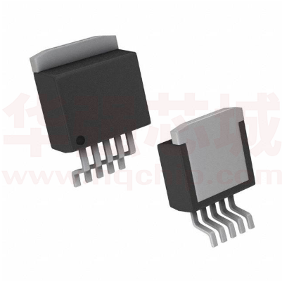
TO263-3L / TO220-3L
(MIC39300-x.x Fixed only)
3A minimum guaranteed output current
500mV typical dropout at 3A
Ideal for 3.0V to 2.5V conversion
Ideal for 2.5V to 1.8V or 1.5V conversion
1% initial accuracy
Low ground current
Current limiting and thermal shutdown
Reversed-battery protection
Reversed-leakage protection
Fast transient response
TTL/CMOS compatible enable pin => MIC39301
Error flag output - MIC39301 only
Adjustable version - MIC39302 only
TO-263 and TO-220 packaging
Moisture Sensitivity Level 3
1. In
2. Gnd
3. Out
1
3
1
3
TO263-5L / TO220-5L
(MIC39301-x.x & MIC39302 only)
1
5
1.
2.
3.
4.
5.
En
In
Gnd
Out
Flg or Adj
1
5
PIN DESCRIPTION
APPLICATIONS
CMOS-compatible control input.
Enable
(Input)
LDO linear regulator for PC add-in cards
High-efficiency linear power supplies
Multimedia and PC processor supplies
SMPS post regulator
Low-voltage microcontrollers
StrongARM™ processor supply
Logic high = enable, logic
Logic low or open = Shutdown
IN
Supply (Input): +16V maximum supply
GND
Ground pin and TAB are internally connected.
OUT
Regulator Output
FLG
Flag (Output): Open-collector error flag output.
ADJ
Adjustment Input: Feedback input.
ORDERING INFORMATION
DESCRIPTION
The MIC39300,MIC39301 and MIC39302 are 3.0A
low-dropout linear voltage regulators that provide
a low voltage, high-current output with a
minimum of external components.
The MIC39300/1 offers extremely low dropout
(typically 400mV at 3.0A) and low ground current
(typically 36mA at 3.0A).
Device
MIC39300S- X.X
MIC39300T-X.X
MIC39301S-X.X
MIC39301T-X.X
MIC39302S-Adj
MIC39302T-Adj
Marking
MIC39300-X.X
MIC39300-X.X
MIC39301-X.X
MIC39301-X.X
MIC39302
MIC39302
Package
TO-263
TO-220
TO-263
TO-220
TO-263
TO-220
* X.X = Fixed Vout = 1.5V, 1.8V, 2.5V, 3.3V, 5.0V
The MIC39300/1/2 is ideal for PC add-in cards that need to convert from standard 5V or 3.3V down to
new, lower core voltages. A guaranteed maximum dropout voltage of 500mV over all operating conditions
allows the MIC39300/1/2 to pro-vide 2.5V from a supply as low as 3V.
The MIC39300/1/2 also has fast transient response for heavy switching applications.The device requires
only 47F of output capacitance to maintain stability and achieve fast transient responseThe MIC39300/1 is
fully protected with over current limiting,thermal shutdown, reversed-battery protection, reversed-leakage
protection, and reversed-lead insertion. The MIC39301 offers a TTL-logic compatible enable pin and an
error flag that indicates under voltage and over current conditions. Offered in fixed voltages, the
MIC39300/1/2 comesin the TO-220 and TO-263 packages and is an ideal upgrade to older, NPN-based
linear voltage regulators.
http://www.hgsemi.com.cn
1
2018 AUG
�MIC39300/39301/39302
Typical Application Circuit
MIC39300
MIC39301
MIC39302
Absolute Maximum Ratings (Note 1)
Supply Voltage (VIN) : –20V to +20V
Enable Voltage (VEN) : +20V
Storage Temperature (TS) : –65°C to +150°C
Lead Temperature (soldering, 5 sec) : 260°C
ESD, Note 3
Operating Ratings (Note 2)
Supply Voltage (VIN) : +2.25V to +16V
Enable Voltage (VEN) : +16V
Maximum Power Dissipation (PD(max)) Note 4
Junction Temperature (TJ) : –40°C to +125°C
Package Thermal Resistance
TO-263(θJC) : 5°C/W
TO-220(θJC) : 2°C/W
http://www.hgsemi.com.cn
2
2018 AUG
�MIC39300/39301/39302
Block Diagram
MIC39300 Fixed (1.5V,1.8V,2.5V,3.3V,5.0V)
MIC39301 Fixed with flag and enable
MIC39302 Adjustable
http://www.hgsemi.com.cn
3
2018 AUG
�MIC39300/39301/39302
550
http://www.hgsemi.com.cn
4
2018 AUG
�MIC39300/39301/39302
Note
Note
Note
Note
Note
Note
Note
Note
Note
1. Exceeding the absolute maximum ratings may damage the device.
2. The device is not guaranteed to function outside its operating rating.
3. Devices are ESD sensitive. Handling precautions recommended.
4. P D(max) = (TJ(max) – TA) θJA, where θJA depends upon the printed circuit layout. See “Applications Information.”
5.Vout temperature coefficient is ∆VOUT(worst case) (TJ(max) – TJ(min)) where T J(max) is +125℃ and TJ(min) is 0℃
6. V DO = V IN – VOUT when V OUT decreases to 99% of its nominal output voltage with V IN = V OUT + 1V.
7. I GND is the quiescent current. IIN = I GND + IOUT.
8. V EN 0.8V, V IN 8V, and V OUT = 0V
9. For a 2.5V device, V IN = 2.250V (device is in dropout).
Note 10.VREF ≤ VOUT ≤ (VIN – 1V), 2.25V ≤ VIN ≤ 16V, 10mA ≤ IL ≤ 3A, TJ = TMAX.
TYPICAL PERFORMANCE CHARACTERISTICS
http://www.hgsemi.com.cn
5
2018 AUG
�MIC39300/39301/39302
http://www.hgsemi.com.cn
6
2018 AUG
�MIC39300/39301/39302
APPLICATION INFORMATION
The MIC39300/1 is a high-performance low-dropout voltage regulator suitable for moderate to high-current voltage
regu-lator applications. Its 500mV dropout voltage at full load makes it especially valuable in battery-powered
systems and as a high-efficiency noise filter in post-regulator applications. Unlike older NPN-pass transistor
designs, where the mini-mum dropout voltage is limited by the base-to-emitter voltage drop and collector-toemitter saturation voltage, dropout per-formance of the PNP output of these devices is limited only by the low V CE
saturation voltage.A trade-off for the low dropout voltage is a varying base drive requirement. The MIC39300/1/2
regulator is fully protected from damage due to fault conditions. Current limiting is provided. This limiting is linear
output current during overload conditions is constant. Thermal shutdown disables the device when the die
temperature exceeds the maximum safe operating tem-perature. Transient protection allows device (and load) survival even when the input voltage spikes above and below nominal. The output structure of these regulators allows
voltages in excess of the desired output voltage to be applied without reverse current flow.
Thermal Design
Linear regulators are simple to use. The most complicated design parameters to consider are thermal
characteristics.Thermal design requires four application-specific param-eters:
•Maximum ambient temperature (T A)
•Output Current (I OUT)
•Output Voltage (V OUT)
•Input Voltage (V IN)
•Ground Current (I GND)
Calculate the power dissipation of the regulator from these numbers and the device parameters from this
datasheet,where the ground current is taken from the data sheet.
PD = (V IN – VOUT) IOUT + VIN·IGND
The heat sink thermal resistance is determined by:
θSA=(TJMAX-TA)/PD -(θJC+θCS)
where TJ (max) 125 ℃ and θCS is between 0℃ and 2℃/W.
The heat sink may be significantly reduced in applications where the minimum input voltage is known and is large
compared with the dropout voltage. Use a series input resistor to drop excessive voltage and distribute the heat
between this resistor and the regulator. The low dropout properties of Taejin regulators allow signifi-cant reductions
in regulator power dissipation and the asso-ciated heat sink without compromising performance. When this
technique is employed, a capacitor of at least 1.0F is needed directly between the input and regulator ground.Refer
to Application Note 9 for further details and examples on thermal design and heat sink specification.
Output Capacitor
The MIC39300/1/2 requires an output capacitor to maintain stability and improve transient response. Proper capacitor
selection is important to ensure proper operation. The MIC39300/1/2 output capacitor selection is dependent upon
the ESR (equivalent series resistance) of the output capacitor to maintain stability. When the output capacitor is 47F
or greater, the output capacitor should have less than 1 of ESR. This will improve transient response as well as
promote stability. Ultralow ESR capacitors, such as ceramic chip capacitors may promote instability. These very low
ESR levels may cause an oscillation and/or underdamped tran-sient response. A low-ESR solid tantalum capacitor
works extremely well and provides good transient response and stability over temperature. Aluminum electrolytics can
also be used, as long as the ESR of the capacitor is < 1.The value of the output capacitor can be increased without
limit. Higher capacitance values help to improve transient response and ripple rejection and reduce output noise.
Input Capacitor
An input capacitor of 1F or greater is recommended when the device is more than 4 inches away from the bulk ac
supply capacitance, or when the supply is a battery. Small, surface-mount, ceramic chip capacitors can be used for
the bypass-ing. Larger values will help to improve ripple rejection by bypassing the input to the regulator, further
improving the integrity of the output voltage.Transient Response and 3.3V.
Fig 1. Capacitor Requirements
http://www.hgsemi.com.cn
7
2018 AUG
�MIC39300/39301/39302
Minimum Load Current
The MIC39300/1/2 regulator is specified between finite loads.
If the output current is too small, leakage currents dominate and the output voltage rises.
A 10mA minimum load current is necessary for proper regulation.
Transient Response and 3.3V to 2.5V Conversion
The MIC39300/1/2 has excellent transient response to varia-tions in input voltage and load current. The device has
been designed to respond quickly to load current variations and input voltage variations. Large output capacitors are
not required to obtain this performance. A standard 47F output capacitor, preferably tantalum, is all that is required.
Larger values help to improve performance even further.By virtue of its low-dropout voltage, this device does not
saturate into dropout as readily as similar NPN-based de-signs. When converting from 3.3V to 2.5V, the NPN-based
regulators are already operating in dropout, with typical dropout requirements of 1.2V or greater. To convert down to
2.5V without operating in dropout, NPN-based regulators require an input voltage of 3.7V at the very least. The
MIC39300/1/2 regulator will provide excellent performance with an input as low as 3.0V. This gives the PNP-based
regulators a distinct advantage over older, NPN-based linear regulators.
Error Flag
The MIC39301 version features an error flag circuit which monitors the output voltage and signals an error condition
when the voltage drops 5% below the nominal output voltage. The error flag is an open-collector output that can sink
10mA during a fault condition.Low output voltage can be caused by a number of problems, including an overcurrent
fault (device in current limit) or low input voltage. The flag is inoperative during overtemperature shutdown.
Enable Input
The MIC39301 version features an enable input for on/off control of the device. Its shutdown state draws “zero” current
(only microamperes of leakage). The enable input is TTL/ CMOS compatible for simple logic interface, but can be
connected to up to 20V. When enabled, it draws approxi-mately 15A.
Adjustable Regulator Design
The MIC39302 allows programming the output voltage any-where bet ween 1.25V and the 16V maximum operating
rating of the family. Two resistors are used. Resistors can be quite large, up to 1MΩ, because of the very high input
impedance and low bias current of the sense comparator: The resistor values are calculated by : R1=R2(Vout/1.250-
1)
Where VO is the desired output voltage. Figure 1 shows component definition. Applications with widely varying load
currents may scale the resistors to draw the minimum load current required for proper operation (see below).
http://www.hgsemi.com.cn
8
2018 AUG
�