UMW
R
UMW AO3402A
UMW AO3402A N-Channel MOSFET
V(BR)DSS
ID
RDS(on)MAX
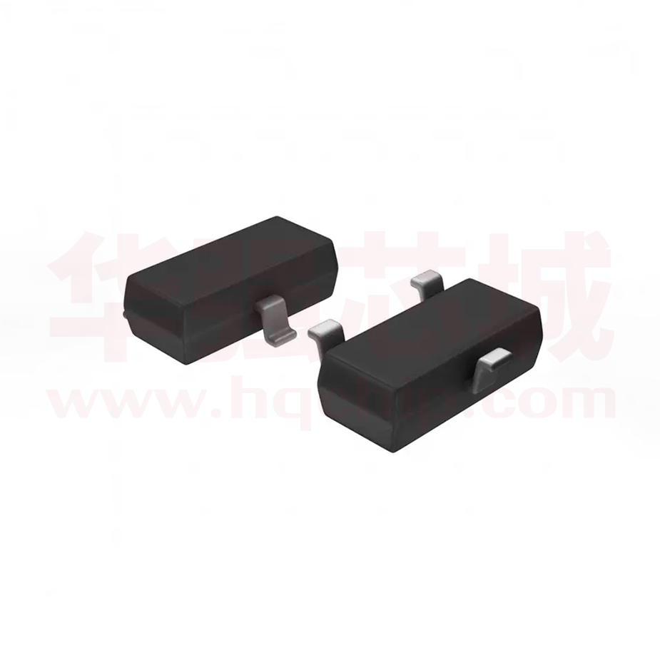
SOT-23
55 mΩ@10V
4A
70 mΩ@4.5V
30V
110 mΩ@2.5V
DESCRIPTION
1. GATE
The 3402 uses advanced trench technology to provide excellent
2. SOURCE
3. DRAIN
RDS(ON) , low gate charge and operation with gate voltage as low as 2.5V.
This device is suitable for use as a load switch or in PWM application.
FEATURES
z Lead free product is acquired
z Surface mount package
APPLICATION
z Load Switch and in PWM applications
MARKING
Equivalent Circuit
A29T
Maximum ratings (Ta=25℃ unless otherwise noted)
Parameter
Symbol
Value
Unit
Drain-Source Voltage
VDS
30
V
Gate-Source Voltage
VGS
±12
V
Continuous Drain Current
ID
4
A
Pulsed Drain Current (note 1)
IDM
15
A
Power Dissipation
PD
0.35
W
RθJA
357
℃/W
Junction Temperature
TJ
150
℃
Storage Temperature
TSTG
-55~+150
℃
Thermal Resistance from Junction to Ambient (note 2)
www.umw-ic.com
1
友台半导体有限公司
�UMW
R
UMW AO3402A
Ta =25 ℃ unless otherwise specified
Parameter
Symbol
Test Condition
Min
Typ
Max
Unit
STATIC CHARACTERISTICS
Drain-source breakdown voltage
V (BR)DSS
VGS = 0V, ID =250µA
Zero gate voltage drain current
IDSS
VDS =24V,VGS = 0V
Gate-body leakage current
IGSS
VGS =±12V, VDS = 0V
VGS(th)
VDS =VGS, ID =250µA
Gate threshold voltage (note 3)
Drain-source on-resistance (note 3)
RDS(on)
30
V
1
µA
100
nA
1.4
V
VGS =10V, ID =4A
55
mΩ
VGS =4.5V, ID =3A
70
mΩ
VGS =2.5V, ID =2A
110
mΩ
Forward transconductance (note 3)
gFS
VDS =15V, ID =4A
Diode forward voltage (note 3)
VSD
IS=1A, VGS = 0V
0.6
8
S
1
V
DYNAMIC CHARACTERISTICS (note 4)
Input capacitance
Ciss
Output capacitance
Coss
Reverse transfer capacitance
Crss
Gate resistance
Rg
VDS =15V,VGS =0V,f =1MHz
VDS =0V,VGS =0V,f =1MHz
390
pF
54.5
pF
41
Pf
3
Ω
3.3
ns
SWITCHING CHARACTERISTICS (note 4)
Turn-on delay time
Turn-on rise time
Turn-off delay time
td(on)
tr
VGS=10V,VDS=15V,
1
ns
td(off)
RL=3.75Ω,RGEN=6Ω
21.7
ns
Turn-off fall time
tf
2.1
ns
Total gate charge
Qg
4.34
nC
Gate-source Charge
Qgs
0.6
nC
Gate-drain Charge
Qgd
1.38
nC
1.2
ns
6.3
nC
Body diode reverse recovery time
Body diode reverse recovery charge
t.
Qrr
VDS =15V,VGS =4.5V,ID =4A
IF=4A,dI/dt=100A/µs
Notes :
1. Repetitive rating : Pulse width limited by junction temperature.
2. Surface mounted on FR4 board , t≤10s.
3. Pulse Test : Pulse Width≤80µs, Duty Cycle≤0.5%.
4. Guaranteed by design, not subject to producting.
www.umw-ic.com
2
友台半导体有限公司
�
很抱歉,暂时无法提供与“UMW AO3402A”相匹配的价格&库存,您可以联系我们找货
免费人工找货- 国内价格
- 5+0.23800
- 20+0.21700
- 100+0.19600
- 500+0.17500
- 1000+0.16520
- 2000+0.15820
