UMW
R
UMW SI2310A
N-Channel Power MOSFET
■ Features
SOT–23
● Simple Drive Requirement
● Small Package Outline
● Surface Mount Device
1. GATE
2. SOURCE
MARKING
3. DRAIN
D
G
MS10
S
■ Absolute Maximum Ratings Ta = 25℃
Parameter
Drain-Source Voltage
Gate-Source Voltage
Continuous Drain Current
Symbol
Rating
Unit
VD S
60
V
VGS
±20
V
TA=25 ℃
ID
TA=70℃
Pulsed Drain Current *
Power Dissipation
TA=25℃
Junction and Storage Temperature Range
A
I DM
10
PD
1.38
W
0.01
W/℃
90
℃/W
-55 to 150
℃
Linear Derating Factor
Thermal Resistance.Junction-to-ambient
3
2.3
RthJa
TJ ,
TSTG
* 2.Pulse width ≤300us , duty cycle≤ 2%.
www.umw-ic.com
1
友台半导体有限公司
�UMW
R
UMW SI2310A
■ Electrical Characteristics Ta = 25℃
Parameter
Symbol
Drain-Source Breakdown Voltage
VDSS
Zero Gate Voltage Drain Current
IDSS
Gate-Body leakage current
Testconditons
ID =250μA, VGS=0V
60
25
VGS(th)
V DS =V GS ID=-250μA
Static Drain-Source On-Resistance
RDS(ON)
1
nA
3
V
90
V GS =4.5V, I D=2A
120
5
Input Capacitance
Ciss
Output Capacitance
C oss
490
Reverse Transfer Capacitance
Crss
40
Total Gate Charge
Qg
6
Gate Source Charge
Q gs
Gate Drain Charge
Q gd
3
Turn-On DelayTime
tD(on)
6
Turn-On Rise Time
tr
Turn-Off DelayTime
tD(off)
V GS =0V, VD S=25V, f=1MHz
VDS=48V, ID=3A ,VGS=4.5V
V GS =10V, V DS=30V,ID=1A RD=30
Ω,RG EN=3.3Ω
μA
±100
V GS =10V, ID=3A
V DS =5V, I D=3A
Unit
V
10
Gate Threshold Voltage
mΩ
S
780
55
pF
10
1.6
nC
5
ns
16
Turn-Off Fall Time
tf
Body Diode Reverse Recovery Time
t rr
IS =3A,dI/dt=100A/μs
25
Body Diode Reverse Recovery Charge
Q rr
IS =3A, dI /dt=100A/μs
26
Diode Forward Voltage
V SD
IS =1.2A,V GS =0V
www.umw-ic.com
Max
V DS =48, V GS =0V ,TJ=70℃
V DS =0V, V GS=±20V
g FS
Typ
V DS =60V, VG S=0V
IGSS
Forward Transconductance
Min
3
2
nC
1.2
V
友台半导体有限公司
�UMW
R
UMW SI2310A
10
10
8
ID , Drain Current (A)
ID , Drain Current (A)
8
10V
7.0V
5.0V
4.5V
o
T A = 150 C
10V
7.0V
5.0V
4.5V
T A =25 o C
6
V G = 3.0 V
4
2
6
V G = 3.0 V
4
2
0
0
0
1
3
2
4
0
5
1
2
3
4
5
V DS , Drain-to-Source Voltage (V)
V DS , Drain-to-Source Voltage (V)
Fig 1. Typical Output Characteristics
Fig 2. Typical Output Characteristics
105
2.0
ID=2A
99
ID=3A
V G =10V
1.8
o
T A =25 C
Normalized R DS(ON)
RDS(ON) (mΩ )
1.6
93
87
1.4
1.2
1.0
81
0.8
0.6
75
2
6
4
8
-50
10
0
50
100
150
T j , Junction Temperature ( o C)
V GS , Gate-to-Source Voltage (V)
Fig 3. On-Resistance v.s. Gate Voltage
Fig 4. Normalized On-Resistance
v.s. Junction Temperature
1.4
3
Normalized VGS(th) (V)
1.2
IS(A)
2
o
o
T j =150 C
T j =25 C
1
1.0
0.8
0.6
0.4
0
0
0.2
0.4
0.6
0.8
1
-50
1.2
V SD , Source-to-Drain Voltage (V)
Fig 5. Forward Characteristic of
50
100
150
Fig 6. Gate Threshold Voltage v.s.
Junction Temperature
Reverse Diode
www.umw-ic.com
0
T j , Junction Temperature ( o C)
3
友台半导体有限公司
�UMW
R
UMW SI2310A
f=1.0MHz
1000
ID=3A
12
C iss
V DS = 30 V
V DS =38V
V DS =48V
10
C (pF)
VGS , Gate to Source Voltage (V)
14
8
100
6
C oss
C rss
4
2
10
0
0
3
9
6
12
1
15
5
Q G , Total Gate Charge (nC)
9
13
17
21
25
29
V DS , Drain-to-Source Voltage (V)
Fig 7. Gate Charge Characteristics
Fig 8. Typical Capacitance Characteristics
1
100.000
Normalized Thermal Response (Rthja)
Duty factor=0.5
10.000
100us
1.000
ID (A)
1ms
10ms
0.100
100ms
1s
DC
T A =25 o C
Single Pulse
0.010
0.2
0.1
0.1
0.05
PDM
0.01
t
0.01
T
Single Pulse
Duty factor = t/T
Peak Tj = PDM x Rthja + Ta
Rthja = 270℃
℃ /W
0.001
0.0001
0.001
0.1
1
10
100
0.01
0.1
1
10
100
1000
t , Pulse Width (s)
V DS , Drain-to-Source Voltage (V)
Fig 9. Maximum Safe Operating Area
www.umw-ic.com
0.001
1000
Fig 10. Effective Transient Thermal Impedance
4
友台半导体有限公司
�
很抱歉,暂时无法提供与“UMW SI2310A”相匹配的价格&库存,您可以联系我们找货
免费人工找货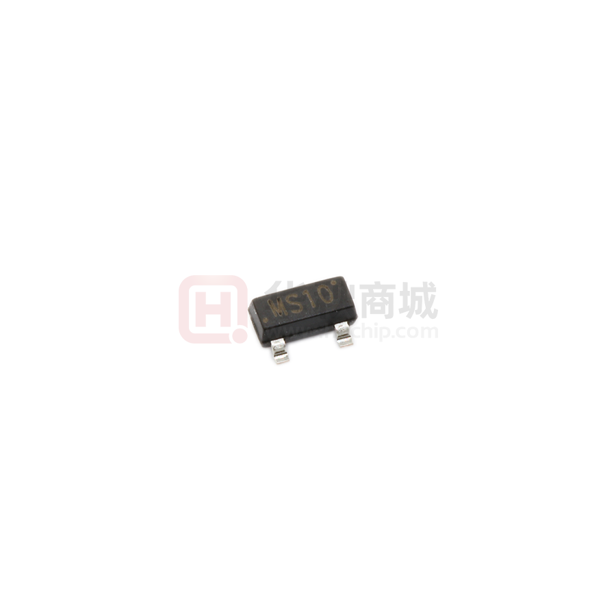


 工商网监
湘ICP备2023018690号
工商网监
湘ICP备2023018690号

