UMW
R
UMW IRLML6402
P-Channel Enhancement MOSFET
■ Features
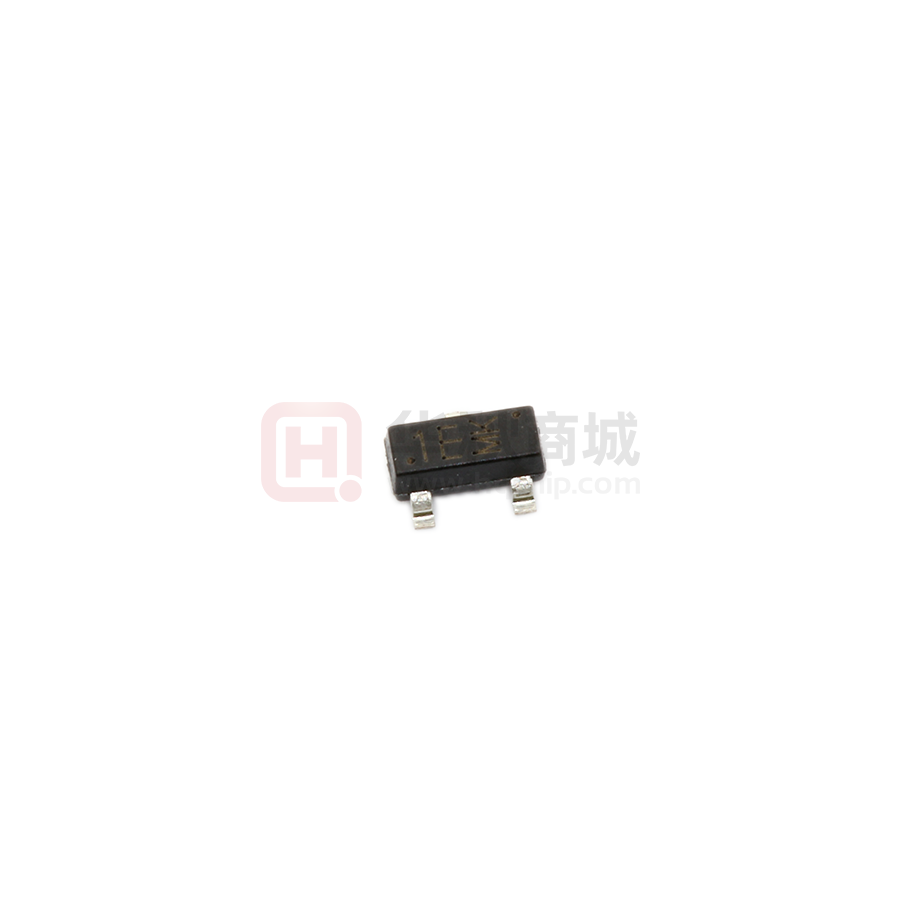
SOT–23
● Ultra low on-resistance.
● P-Channel MOSFET.
● SOT-23 Footprint.
● Low profile(<1.1mm).
● Available in tape and reel.
1. BASE
● Fast switching.
2. EMITTER
3. COLLECTOR
MARKING
1E MK
■ Absolute Maximum Ratings Ta = 25℃
Parameter
Symbol
Rating
Drain-Source Voltage
VDS
-20
Gate-Source Voltage
VGS
±12
Continuous Drain Current VGS=4.5V @ TA=25℃
Continuous Drain Current
ID
VGS=4.5V@ TA=70℃
Pulsed Drain Current
a
Power Dissipation
@ TA=25℃
Power Dissipation
@ TA=70℃
Single Pulse Avalanche Energy
b
Thermal Resistance.Junction- to-Ambient
IDM
PD
EAS
RthJA
Linera Derating Factor
Unit
V
-3.7
-2.2
A
-30
1.3
0.8
11
W
mJ
100
℃/W
0.01
W/℃
Junction Temperature
TJ
150
Junction and Storage Temperature Range
Tstg
-55 to 150
℃
Notes:
a.Repetitive Rating :Pulse width limited by maximum junction temperature
b.Starting TJ=25℃, L=1.65mH, RG=25Ω, IAS=-3.7A
www.umw-ic.com
1
友台半导体有限公司
�UMW
R
UMW IRLML6402
P-Channel Enhancement MOSFET
■ Electrical Characteristics Ta = 25℃
Parameter
Test conditions
Symbol
Drain-source Breakdown voltage
Zero Gate Voltage Drain Current
ce leadage
VDSS
IDSS
I
e
Static drain-source on- resistance
Forward Transconductance
V
= 0V
VDS = -20 V, V
ID
= 0V
VDS = -20 V, V
= 0V, TJ
V
V
RDS(on)
V
= -4.5V
0.050
ID= -3.1A, V
= -2.5V
0.080 0.135
Ciss
VDS = -10 V,
V
Reverse transfer capacitance
Crss
f= 1MHz
-0.40
gd
td(on)
Rise time
tr
Turn-off delay time
td(off)
= 0 V,
VDS = -10V ,V
= -5.0 V , ID
ID
8.0
12
1.2
1.8
2.8
4.2
VDD= -10 V,
48
RD
Ω
588
Ω
381
tf
R
TJ=25℃, IF = -1.0 A,
μs
Pulsed source curren
ISM
MOSFET symbo
l showing the
integral reverse
p-n junction diode
Diode forward voltage
VSD
TJ=25℃,V
IS
pF
nC
350
trr
Continuous source current
Ω
110
Reverse recovery time
rr
nA
V
145
Fall time
Reverse recovery charge
-0.55
S
g
rain Charge
tit
-25
℃
ID
Coss
Turn-on delay time
V
±100
VDS = -10 V, ID
Unit
-1.0
, ID
gfs
gs
Max
-20
=±12V
Input capacitance
ce Charge
Typ
VDS = V
Output capacitance
e
Min
ns
43
11
ns
nC
D
-1.3
A
G
= 0 V, IS = -1.0 A
S
-22
-1.2
V
lse width limited by max.junction temperature.
e width ≤ 400μs, Duty cycle ≤
www.umw-ic.com
2
友台半导体有限公司
�UMW
R
UMW IRLML6402
P-Channel Enhancement MOSFET
■ Typical Characterisitics
100
100
VGS
-7.00V
-5.00V
-4.50V
-3.50V
-3.00V
-2.70V
-2.50V
BOTTOM -2.25V
-I D , Drain-to-Source Current (A)
-I D , Drain-to-Source Current (A)
10
-2.25V
1
0.1
20µs PULSE WIDTH
TJ = 25 °C
1
10
-VDS , Drain-to-Source Voltage (V)
10
-2.25V
1
0.1
100
Fig 1. Typical Output Characteristics
R DS(on) , Drain-to-Source On Resistance
(Normalized)
-I D , Drain-to-Source Current (A)
2.0
TJ = 25 ° C
TJ = 150 ° C
V DS = -15V
20µs PULSE WIDTH
3.0
4.0
5.0
6.0
7.0
-VGS , Gate-to-Source Voltage (V)
8.0
1
10
-VDS , Drain-to-Source Voltage (V)
100
ID = -3.7A
1.5
1.0
0.5
0.0
-60 -40 -20
VGS = -4.5V
0
20
40
60
80 100 120 140 160
TJ , Junction Temperature ( °C)
Fig 3. Typical Transfer Characteristics
www.umw-ic.com
20µs PULSE WIDTH
TJ = 150 °C
Fig 2. Typical Output Characteristics
100
10
2.0
VGS
-7.00V
-5.00V
-4.50V
-3.50V
-3.00V
-2.70V
-2.50V
BOTTOM -2.25V
TOP
TOP
Fig 4. Normalized On-Resistance
3
友台半导体有限公司
�UMW
R
UMW IRLML6402
P-Channel Enhancement MOSFET
■ Typical Characterisitics
1000
-VGS , Gate-to-Source Voltage (V)
800
C, Capacitance(pF)
10
VGS = 0V,
f = 1 MHZ
Ciss = Cgs + Cgd, Cds SHORTED
Crss = Cgd
Coss = Cds + Cgd
Ciss
600
400
Coss
200
Crss
0
VDS =-10V
8
6
4
2
0
1
10
ID = -3.7A
100
FOR TEST CIRCUIT
SEE FIGURE 13
0
3
VDS, Drain-to-Source Voltage (V)
9
12
Fig 6. Typical Gate Charge Vs.
Gate-to-Source Voltage
Fig 5. Typical Capacitance Vs.
Drain-to-Source Voltage
100
100
OPERATION IN THIS AREA LIMITED
BY RDS(on)
-II D , Drain Current (A)
-ISD , Reverse Drain Current (A)
6
QG , Total Gate Charge (nC)
10
.
TJ = 150 ° C
1
TJ = 25 ° C
0.1
0.2
0.6
0.8
1.0
1ms
1
10ms
0.1
0.1
1.2
-VSD ,Source-to-Drain Voltage (V)
1
10
-VDS , Drain-to-Source Voltage (V)
100
Fig 8. Maximum Safe Operating Area
Fig 7. Typical Source-Drain Diode
Forward Voltage
www.umw-ic.com
100us
TC = 25 ° C
TJ = 150 ° C
Single Pulse
V GS = 0 V
0.4
10us
10
4
友台半导体有限公司
�UMW
R
UMW IRLML6402
P-Channel Enhancement MOSFET
■ Typical Characterisitics
25
EAS , Single Pulse Avalanche Energy (mJ)
-ID , Drain Current (A)
4.0
3.0
2.0
1.0
0.0
25
50
75
100
125
TC , Case Temperature ( ° C)
150
Fig 9. Maximum Drain Current Vs.
Case Temperature
ID
-1.7A
-3.0A
BOTTOM -3.7A
TOP
20
15
10
5
0
25
50
75
100
125
Starting TJ , Junction Temperature ( °C)
150
Fig 10. Maximum Avalanche Energy
Vs. Drain Current
Thermal Response (Z thJA )
1000
100
D = 0.50
0.20
0.10
10
0.05
PDM
0.02
0.01
t1
SINGLE PULSE
(THERMAL RESPONSE)
1
0.1
0.00001
t2
Notes:
1. Duty factor D = t 1 / t 2
2. Peak T J = P DM x Z thJA + TA
0.0001
0.001
0.01
0.1
t1 , Rectangular Pulse Duration (sec)
1
10
Fig 11. Maximum Effective Transient Thermal Impedance, Junction-to-Ambient
www.umw-ic.com
5
友台半导体有限公司
�UMW
R
UMW IRLML6402
P-Channel Enhancement MOSFET
R DS(on) , Drain-to -Source Voltage ( Ω )
0.14
0.12
0.10
0.08
Id = -3.7A
0.06
0.04
0.02
2.0
3.0
4.0
5.0
6.0
7.0
-V GS, Gate -to -Source Voltage ( V )
0.20
VGS = -2.5V
0.16
0.12
0.08
VGS = -4.5V
0.04
0.00
0
5
10
15
20
25
30
-I D , Drain Current ( A )
Fig 12. Typical On-Resistance Vs.
Gate Voltage
www.umw-ic.com
R DS ( on ) , Drain-to-Source On Resistance ( Ω )
■ Typical Characterisitics
Fig 13. Typical On-Resistance Vs.
Drain Current
6
友台半导体有限公司
�


 工商网监
湘ICP备2023018690号
工商网监
湘ICP备2023018690号
