UMW
R
UMW SI2302A
N-Channel Enhancement MOSFET
■ Features
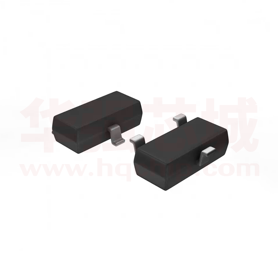
SOT–23
● VDS=20V
● RDS(on)= 85mΩ@VGS=4.5V ,ID=3.6A
● RDS(on)= 115mΩ@VGS=2.5V ,ID=3.1A
■ Marking
1. GATE
2. SOURCE
G
1
S
2
3. DRAIN
3
D
■ Absolute Maximum Ratings Ta = 25℃
Parameter
Symbol
Rating
Drain-Source Voltage
VDS
20
Gate-Source Voltage
VGS
±8
Continuous Drain Current
*1
Ta=25℃
ID
Ta=70℃
Pulsed Drain Current
Power Dissipati
Thermal Resistance.Junction- to-Ambient
IDM
Ta=25℃
PD
Ta=70℃
*1
RthJA
*2
Junction Temperature
Storage Temperature Range
Unit
V
2.8
2.2
A
10
1.25
0.8
100
166
TJ
150
Tstg
-55 to 150
W
℃/W
℃
Notes:
*1.Surface Mounted on FR4 Board, t ≤ 5 sec.
*2.Surface Mounted on FR4 Board.
www.umw-ic.com
1
友台半导体有限公司
�UMW
R
UMW SI2302A
N-Channel Enhancement MOSFET
■ Electrical Characteristics Ta = 25℃
Parameter
Drain-Source Breakdown Voltage
Zero Gate Voltage Drain Current
Gate-Body Leakage Current
Gate Threshold Voltage
Static Drain-Source On-Resistance
Symbol
VDSS
IDSS
IGSS
VGS(th)
RDS(On)
Forward Transconductance *
gfs
Input Capacitance
Ciss
Output Capacitance
Coss
Reverse Transfer Capacitance
Crss
Total Gate Charge
Qg
Gate-Source Charge
Qgs
Gate-Drain Charge
Qgd
Turn-On DelayTime
td(on)
Turn-On Rise Time
tr
Turn-Off DelayTime
td(off)
Turn-Off Fall Time
Continuous Source Current (Diode Conduction)
Diode Forward Voltage
Test Conditions
ID=250μA, VGS=0V
Typ
Max
20
Unit
V
VDS=20V, VGS=0V
1
VDS=20V, VGS=0V ,TJ=55 ℃
10
μA
±100
nA
0.95
1.9
V
VGS=4.5V, ID=3.6A
45
85
VGS=2.5V, ID=3.1A
70
115
VDS=0V, VGS=±8V
VDS=VGS , ID=250μA
VDS=5V,ID=3.6A
0.62
8
mΩ
S
300
VGS=0V, VDS=10V, f=1MHz
pF
120
80
4
VDS=10V,VGS=4.5V,ID=3.6A
10
nC
0.65
1.5
VGS=4.5V, VDS=10V, RL=5.5Ω,RGEN=6Ω
ID=3.6A
tf
7
15
55
80
16
60
10
25
1.6
IS
VSD
Min
Is=1.6A ,VGS=0V
0.76
ns
A
1.2
V
* Pulse test: PW ≤300us duty cycle≤ 2%
www.umw-ic.com
2.
友台半导体有限公司
�R
UMW
UMW SI2302A
N-Channel Enhancement MOSFET
■ Typical Characterisitics
Output Characteristics
10
Transfer Characteristics
10
VGS = 5 thru 2.5 V
8
2V
I D – Drain Current (A)
I D – Drain Current (A)
8
6
4
2
1.5 V
0, 0.5, 1 V
6
TC = 125 。
C
4
。
2
25 C
。
–55 C
0
0
0
1
2
3
4
5
0
0.5
VDS – Drain-to-Source Voltage (V)
2.0
2.5
Capacitance
1000
0.12
800
C – Capacitance (pF)
r DS(on)– On-Resistance ( Ω )
1.5
VGS – Gate-to-Source Voltage (V)
On-Resistance vs. Drain Current
0.15
1.0
VGS = 2.5 V
0.09
VGS = 4.5 V
0.06
0.03
600
Ciss
400
Coss
200
Crss
0
0
0
2
4
6
8
10
0
Gate Charge
1.8
1.6
4
r DS(on)– On-Resistance ( Ω )
(Normalized)
V GS – Gate-to-Source Voltage (V)
VDS = 10 V
ID = 3.6 A
3
2
1
0
0
1
2
3
4
5
6
12
16
20
On-Resistance vs. Junction Temperature
VGS = 4.5 V
ID = 3.6 A
1.4
1.2
1.0
0.8
0.6
–50
7
0
50
100
150
C)
TJ – Junction Temperature (。
Qg – Total Gate Charge (nC)
www.umw-ic.com
8
VDS – Drain-to-Source Voltage (V)
ID – Drain Current (A)
5
4
3
友台半导体有限公司
�UMW
R
UMW SI2302A
N-Channel Enhancement MOSFET
■ Typical Characterisitics
Source-Drain Diode Forward Voltage
On-Resistance vs. Gate-to-Source Voltage
0.20
r DS(on)– On-Resistance ( Ω )
I S – Source Current (A)
10
TJ = 150。
C
TJ = 25。
C
0.16
0.12
ID = 3.6 A
0.08
0.04
1
0
0.2
0.4
0.6
0.8
1.0
0
1.2
2
VSD – Source-to-Drain Voltage (V)
12
–0.0
10
ID = 250 A
Power (W)
V GS(th) Variance (V)
8
Single Pulse Power
14
0.1
–0.1
–0.2
8
TC = 25。
C
Single Pulse
6
4
–0.3
2
.
–0.4
–50
0
50
100
0
150
0.01
0.10
TJ – Temperature (。
C)
1
1.00
10.00
Time (sec)
Normalized Thermal Transient Impedance, Junction-to-Ambient
2
Normalized Effective Transient
Thermal Impedance
6
VGS – Gate-to-Source Voltage (V)
Threshold Voltage
0.2
4
Duty Cycle = 0.5
0.2
0.1
0.1
0.05
0.02
0.01
10–4
Single Pulse
10–3
10–2
10–1
1
10
30
Square Wave Pulse Duration (sec)
www.umw-ic.com
4
友台半导体有限公司
�
很抱歉,暂时无法提供与“UMW SI2302A”相匹配的价格&库存,您可以联系我们找货
免费人工找货- 国内价格
- 1000+0.06625
- 3000+0.05681