UMW
SMD Type
R
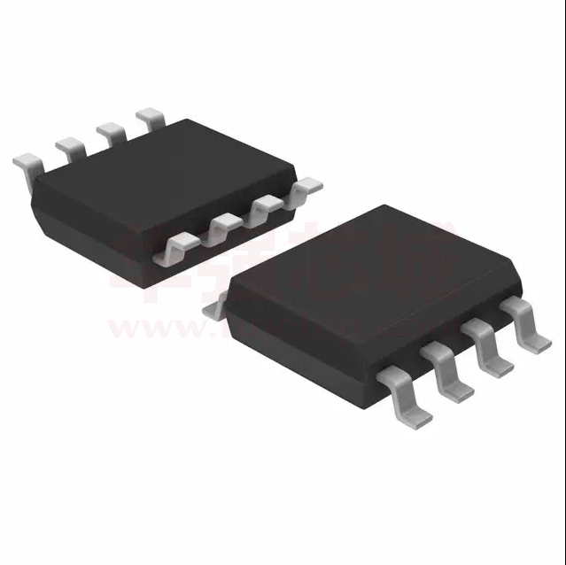
UMW LM393A
Integrate Circuit
Low Power Low Offset Voltage Dual Comparators
Features
Wide Single-Supply Range: 2.0 V to 36 V
Split-Supply Range:
1.0 V to
18 V
Very Low Current Drain Independent of Supply Voltage: 0.4 mA
Low Input Bias Current: 25 nA
Low Input Offset Current: 5.0 nA
Low Input Offset Voltage: 5.0 mV (max)
Input Common Mode Range to Ground Level
Differential Input Voltage Range Equal to Power Supply Voltage
Representative Schematic Diagram
Absolute Maximum Ratings Ta = 25
Parameter
Symbol
Rating
Unit
V
Power Supply Voltage
VCC
+36 or
Input Differential Voltage Range
VIDR
36
V
Input Common Mode Voltage Range
VICR
-0.3 to +36
V
Output Short Circuit-to-Ground
ISC
Continuous
Output Sink Current*
ISink
20
Power Dissipation @ TA = 25
PD
570
Derate above 25
Operating Ambient Temperature Range
Maximum Operating Junction Temperature
Storage Temperature Range
1/R
18
5.7
JA
TA
0 to 70
TJ(max)
150
Tstg
-65 to +150
Vesd
2000
200
mA
mW
mW/
ESD Protection at any Pin
- Human Body Model
- Machine Model
V
* The maximum output current may be as high as 20 mA, independent of the magnitude of VCC,
output short circuits to VCC can cause excessive heating and eventual destruction.
www.umw-ic.com
1
友台半导体有限公司
�UMW
SMD Type
R
UMW LM393A
Integrate Circuit
Electrical Characteristics (VCC = 5.0 V, 0
Parameter
Input Offset Voltage*1
TA
VIO
Testconditons
IIO
IIB
Min
1.0
TA
5.0
TA
70
25
mV
50
nA
250
0
VCC 1.5
0
VCC 2.0
VICR
TA
5.0
nA
400
70
TA = 25
0
Unit
150
TA = 25
TA
Max
9.0
70
TA = 25
0
Input Common Mode Voltage Range *2
Typ
TA = 25
0
Input Bias Current *2
, unless otherwise noted.)
Symbol
0
Input Offset Current
70
70
200
V/mV
Vin = TTL Logic Swing, Vref = 1.4 V,VRL = 5.0 V,
RL = 5.1 k , TA = 25
300
ns
tTLH
VRL = 5.0 V, RL = 5.1 k
1.3
Input Differential Voltage *5
VID
All Vin
Output Sink Current
ISink
Vin
1.0 V, Vin+ = 0 V, VO
1.5 V TA = 25
Output Saturation Voltage
VOL
Vin
1.0 V, Vin+ = 0, ISink
4.0 mA, TA = 25
Voltage Gain
AVOL
Large Signal Response Time
Response Time *4
RL
15 k
0
, VCC = 15 V, TA = 25
Supply Current
IOL
ICC
, TA = 25
TA
s
VCC
GND or V-Supply (if used)
6.0
16
150
V
mA
400
mV
700
70
Vin- = 0 V, Vin+
Output Leakage Current
50
V
1.0 V, VO = 5.0 V, TA = 25
Vin- = 0 V, Vin+ 1.0 V, VO = 30 V,0
70
RL =
Both Comparators, TA = 25
RL =
Both Comparators, VCC = 30 V
0.1
nA
TA
1000
0.4
1.0
mA
2.5
*1. At output switch point, VO=1.4 V, RS = 0Ù with VCC from 5.0 V to 30 V, and over the full input common mode range (0 V to
VCC = -1.5 V).
*2. Due to the PNP transistor inputs, bias current will flow out of the inputs. This current is essentially constant, independent of
the output state, therefore, no loading changes will exist on the input lines.
*3. Input common mode of either input should not be permitted to go more than 0.3 V negative of ground or minus supply.
The upper limit of common mode range is VCC -1.5 V.
*4. Response time is specified with a 100 mV step and 5.0 mV of overdrive. With larger magnitudes of overdrive faster response
times are obtainable.
*5. The comparator will exhibit proper output state if one of the inputs becomes greater than VCC, the other input must remain
within the common mode range. The low input state must not be less than -0.3 V of ground or minus supply.
www.umw-ic.com
2
友台半导体有限公司
�
很抱歉,暂时无法提供与“UMW LM393ADR”相匹配的价格&库存,您可以联系我们找货
免费人工找货- 国内价格
- 5+0.22100
- 20+0.20150
- 100+0.18200
- 500+0.16250
- 1000+0.15340
- 2000+0.14690
