UMW
R
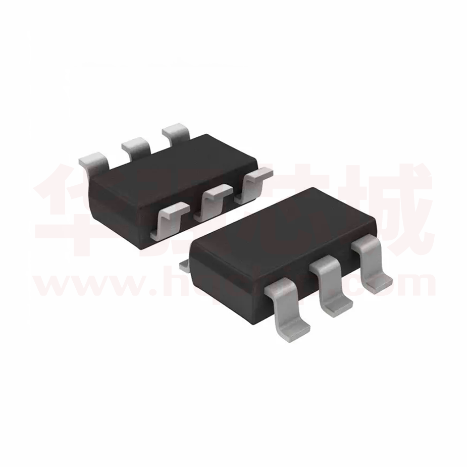
UMW NDC7002N
SOT23-6 Dual N-Channel Enhancement Mode Field Effect Transistor
General Description
Features
0.51A, 50V, RDS(ON) = 2Ω @ VGS=10V
These dual N-Channel enhancement mode power field
effect transistors are produced using Fairchild's
proprietary, high cell density, DMOS technology. This
very high density process has been designed to minimize
on-state resistance, provide rugged and reliable
performance and fast switching. These devices is
particularly suited for low voltage applications requiring a
low current high side switch.
High density cell design for low RDS(ON).
Proprietary SOT23-6 package design using copper lead
frame for superior thermal and electrical capabilities.
High saturation current.
____________________________________________________________________________________________
4
3
5
2
6
1
SOT23-6
Absolute Maximum Ratings T A = 25°C unless otherwise noted
Symbol
Parameter
NDC7002N
Units
VDSS
Drain-Source Voltage
50
V
VGSS
Gate-Source Voltage - Continuous
20
V
ID
Drain Current - Continuous
0.51
A
(Note 1a)
- Pulsed
PD
Maximum Power Dissipation
1.5
(Note 1a)
(Note 1b)
(Note 1c)
TJ,TSTG
Operating and Storage Temperature Range
0.96
W
0.9
0.7
-55 to 150
°C
(Note 1a)
130
°C/W
(Note 1)
60
°C/W
THERMAL CHARACTERISTICS
RθJA
Thermal Resistance, Junction-to-Ambient
RθJC
Thermal Resistance, Junction-to-Case
www.umw-ic.com
1
友台半导体有限公司
�UMW
R
UMW NDC7002N
SOT23-6 Dual N-Channel Enhancement Mode Field Effect Transistor
ELECTRICAL CHARACTERISTICS (TA = 25°C unless otherwise noted)
Symbol
Parameter
Conditions
Min
Typ
Max
Units
OFF CHARACTERISTICS
BVDSS
Drain-Source Breakdown Voltage
VGS = 0 V, ID = 250 µA
IDSS
Zero Gate Voltage Drain Current
VDS = 40 V, VGS = 0 V
50
V
1
µA
500
TJ = 125°C
IGSSF
Gate - Body Leakage, Forward
VGS = 20 V, VDS = 0 V
100
nA
IGSSR
Gate - Body Leakage, Reverse
VGS = -20 V, VDS= 0 V
-100
nA
V
ON CHARACTERISTICS (Note 2)
VGS(th)
Gate Threshold Voltage
VDS = VGS, ID = 250 µA
TJ = 125°C
RDS(ON)
Static Drain-Source On-Resistance
1
1.9
2.5
0.8
1.5
2.2
VGS = 10 V, ID = 0.51 A
TJ = 125°C
VGS = 4.5 V, ID = 0.35 A
1
2
1.7
3.5
1.6
4
1.5
Ω
ID(on)
On-State Drain Current
VGS = 10 V, VDS = 10 V
A
gFS
Forward Transconductance
VDS = 10 V, ID = 0.51 A
400
mS
VDS = 25 V, VGS = 0 V,
f = 1.0 MHz
20
pF
13
pF
5
pF
DYNAMIC CHARACTERISTICS
Ciss
Input Capacitance
Coss
Output Capacitance
Crss
Reverse Transfer Capacitance
SWITCHING CHARACTERISTICS (Note 2)
tD(on)
Turn - On Delay Time
tr
Turn - On Rise Time
VDD = 25 V, ID = 0.25 A,
VGS = 10 V, RGEN = 25 Ω
6
20
6
20
tD(off)
Turn - Off Delay Time
11
20
tf
Turn - Off Fall Time
5
20
Qg
Total Gate Charge
Qgs
Gate-Source Charge
Qgd
Gate-Drain Charge
www.umw-ic.com
VDS = 25 V,
ID = 0.51 A, VGS = 10 V
2
nS
1
nC
0.19
nC
0.33
nC
友台半导体有限公司
�UMW
R
UMW NDC7002N
SOT23-6 Dual N-Channel Enhancement Mode Field Effect Transistor
ELECTRICAL CHARACTERISTICS (TA = 25°C unless otherwise noted)
Symbol
Parameter
Conditions
Min
Typ
Max
Units
DRAIN-SOURCE DIODE CHARACTERISTICS
IS
Maximum Continuous Source Current
0.51
A
ISM
Maximum Pulse Source Current (Note 2)
1.5
A
VSD
Drain-Source Diode Forward Voltage
1.2
V
VGS = 0 V, IS = 0.51 A (Note 2)
0.8
Notes:
1. RθJA is the sum of the junction-to-case and case-to-ambient thermal resistance where the case thermal reference is defined as the solder mounting surface of the drain pins. RθJC is guaranteed by
design while RθCA is determined by the user's board design.
P D (t ) =
T J−TA
R θJ A(t )
=
T J−TA
R θJ C+RθCA(t )
= I 2D (t ) × RDS(ON )
TJ
Typical RθJA for single device operation using the board layouts shown below on 4.5"x5" FR-4 PCB in a still air environment:
o
2
a. 130 C/W when mounted on a 0.125 in pad of 2oz cpper.
b. 140oC/W when mounted on a 0.005 in2 pad of 2oz cpper.
c. 180oC/W when mounted on a 0.0015 in2 pad of 2oz cpper.
1a
1b
1c
Scale 1 : 1 on letter size paper
2. Pulse Test: Pulse Width < 300µs, Duty Cycle < 2.0%.
www.umw-ic.com
3
友台半导体有限公司
�UMW
R
UMW NDC7002N
SOT23-6 Dual N-Channel Enhancement Mode Field Effect Transistor
Typical Electrical Characteristics
1.5
3
8.0 7.0
VGS = 3.5V
6.0
1.2
RDS(on) , NORMALIZED
5.5
5.0
0.9
4.5
0.6
4.0
3.5
0.3
DRAIN-SOURCE ON-RESISTANCE
I D , DRAIN-SOURCE CURRENT (A)
V GS =10V
3.0
5.0
6.0
1.5
2
3
4
, DRAIN-SOURCE VOLTAGE (V)
8.0
10
1
0.3
5
0.6
0.9
I D , DRAIN CURRENT (A)
1.2
1.5
Figure 2. On-Resistance Variation with Gate
Voltage and Drain Current.
2
2.5
V GS = 10V
R DS(on), NORMALIZED
DRAIN-SOURCE ON-RESISTANCE
I D = 0.51A
1.8
R DS(ON), NORMALIZED
7.0
0
1
VDS
DRAIN-SOURCE ON-RESISTANCE
5.5
0.5
Figure 1. On-Region Characteristics.
V GS = 10V
1.6
1.4
1.2
1
0.8
0.6
0.4
-50
2
TJ = 125°C
1.5
25°C
1
-55°C
0.5
-25
0
25
50
75
100
TJ , JUNCTION TEMPERATURE (°C)
125
0
150
0.3
I
Figure 3. On-Resistance Variation with
Temperature.
D
0.6
0.9
, DRAIN CURRENT (A)
1.2
1.5
Figure 4. On-Resistance Variation with Drain
Current and Temperature.
1.2
V DS = 10V
T
J
= -55°C
25°C
125°C
V th, NORMALIZED
1.2
0.9
0.6
0.3
0
1
2
3
4
5
6
V GS , GATE TO SOURCE VOLTAGE (V)
7
8
V DS = V GS
I D = 250µA
1.1
1
0.9
0.8
0.7
-50
-25
0
25
50
75
100
TJ , JUNCTION TEMPERATURE (°C)
125
150
Figure 6. Gate Threshold Variation with
Temperature.
Figure 5. Transfer Characteristics.
www.umw-ic.com
GATE-SOURCE THRESHOLD VOLTAGE
1.5
I D , DRAIN CURRENT (A)
4.5
2
0
0
4.0
2.5
4
友台半导体有限公司
�UMW
R
UMW NDC7002N
SOT23-6 Dual N-Channel Enhancement Mode Field Effect Transistor
1.16
I
D
1.5
1
= 250µA
1.12
1.08
1.04
1
0.96
0.92
0.88
-50
-25
0
25
50
75
100
TJ , JUNCTION TEMPERATURE (°C)
125
TJ = 125°C
-55°C
0.01
Figure 7. Breakdown Voltage Variation with
Temperature.
0.4
0.6
0.8
1
V SD , BODY DIODE FORWARD VOLTAGE (V)
1.2
Figure 8. Body Diode Forward Voltage Variation
with Current and Temperature.
10
100
VDS = 25V
V GS , GATE-SOURCE VOLTAGE (V)
50
C iss
CAPACITANCE (pF)
25°C
0.1
0.001
0.2
150
V GS = 0V
0.5
I S , REVERSE DRAIN CURRENT (A)
BV DSS , NORMALIZED
DRAIN-SOURCE BREAKDOWN VOLTAGE
Typical Electrical Characteristics (continued)
20
C oss
10
C rss
5
f = 1 MHz
2
V GS = 0 V
1
0.1
8
I D = 0.51A
6
4
2
0
0.2
0.5
1
2
5
10
20
50
V DS , DRAIN TO SOURCE VOLTAGE (V)
Figure 9. Capacitance Characteristics.
0
0.2
0.4
0.6
0.8
Q g , GATE CHARGE (nC)
1
1.2
Figure 10. Gate Charge Characteristics.
0.7
V DS = 10V
T
I D , DRAIN CURRENT (A)
0.6
0.5
J
= -55°C
25°C
0.4
125°C
0.3
0.2
0.1
0
0
0.3
V
GS
0.6
0.9
1.2
, GATE TO SOURCE VOLTAGE (V)
1.5
Figure 11. Transconductance Variation with Drain
Current and Temperature.
www.umw-ic.com
5
友台半导体有限公司
�R
UMW
UMW NDC7002N
SOT23-6 Dual N-Channel Enhancement Mode Field Effect Transistor
Typical Thermal Characteristics
0.55
I D , STEADY-STATE DRAIN CURRENT (A)
STEADY-STATE POWER DISSIPATION (W)
1.2
1.1
1a
1
0.9
1b
0.8
1c
4.5"x5" FR-4 Board
0.7
o
TA = 2 5 C
Still Air
0.6
0
0.2
0.4
0.6
0.8
2oz COPPER MOUNTING PAD AREA (in 2 )
1
1a
0.5
1b
0.45 1c
0.4
4.5"x5" FR-4 Board
o
TA = 2 5 C
Still Air
VG S = 1 0 V
0.35
0
Figure 12. SOT23-6 Dual Package Maximum
Steady-State Power Dissipation versus Copper
Mounting Pad Area.
0.025
0.05
0.075
0.1
2
2oz COPPER MOUNTING PAD AREA (in )
0.125
Figure 13. Maximum Steady-State Drain
Current versus Copper Mounting Pad
Area.
3
2
I D , DRAIN CURRENT (A)
1
RD
S(O
N)
LIM
IT
10
0
1m us
s
0.5
10
0.2
10
0.1
V
0.05
GS
0m
ms
s
1s
= 10V
DC
SINGLE PULSE
R θJ A = See Note 1c
0.02
T A = 25°C
0.01
1
2
5
10
20
V DS , DRAIN-SOURCE VOLTAGE (V)
50
70
Figure 14. Maximum Safe Operating Area.
r(t), NORMALIZED EFFECTIVE
TRANSIENT THERMAL RESISTANCE
1
0 .5
D = 0.5
0 .2
0.2
0 .1
R JA (t) = r(t) * R JA
θ
θ
R JA = See Note 1c
θ
0.1
P(pk)
0.05
t1
0.05
0.02
0.01
0.02
0.01
0 .0 0 0 1
www.umw-ic.com
= P * R JA (t)
θ
Duty Cycle, D = t 1 / t 2
A
Single Pulse
0 .001
t2
TJ - T
0 .0 1
0 .1
t 1, TIME (sec)
6
1
10
100
300
友台半导体有限公司
�