LM2591HV
LM2591HV SIMPLE SWITCHER® Power Converter 150-kHz, 1-A Step-Down Voltage Regulator
Features
Description
3.3-V, 5-V, and Adjustable Output Versions
Adjustable Version Output Voltage Range: 1.2 V
to 57 V ±4% Maximum Over Line and Load
Conditions
Specified 1-A Output Load Current
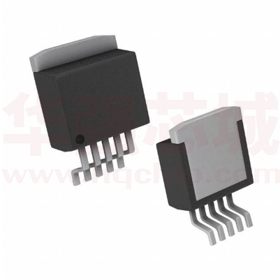
Available in 5-Pin Package
Input Voltage Range Up to 60 V
150-kHz Fixed Frequency Internal Oscillator
ON and OFF Control
Low Power Standby Mode, IQ Typically 90 μA
High Efficiency
Thermal Shutdown and Current-Limit Protection
The LM2591HV series of regulators are monolithic
integrated circuits that provide all the active functions
for a step-down (buck) switching regulator, capable of
driving a 1-A load with excellent line and load
regulation. These devices are available in fixed output
voltages of 3.3 V, 5 V, and an adjustable output
version.
This series of switching regulators is similar to the
LM2590HV, but without some of the supervisory and
control features of the latter.
Requiring a minimum number of external
components, these regulators are simple to use and
include internal frequency compensation, improved
line and load specifications, and a fixed-frequency
oscillator.
Applications
The LM2591HV operates at a switching frequency of
150 kHz, thus allowing smaller sized filter
components than what would be needed with lower
frequency switching regulators. Available in a
standard 5-pin package with several different lead
bend options, and a 5-pin surface mount package.
Simple High-Efficiency Step-Down (Buck)
Regulators
Efficient Preregulator for Linear Regulators
On-Card Switching Regulators
Positive-to-Negative Converters
Device Information(1)
PART
NUMBER
LM2591HV
PACKAGE
BODY SIZE (NOM)
DDPAK/TO-263 (5)
10.18 mm × 8.41 mm
TO-220 (5)
14.986 mm × 10.16 mm
(1) For all available packages, see the orderable addendum at
the end of the data sheet.
Typical Application
Copyright © 2016, Texas Instruments Incorporated
(Fixed Output Voltage Versions)
http://www.hgsemi.com.cn
1
2018 JUN
�LM2591HV
Description (continued)
Other features include a specified ±4% tolerance on output voltage under all conditions of input voltage and
output load conditions, and ±15% on the oscillator frequency. External shutdown is included, featuring typically
90-μA standby current. Self-protection features include a two stage current limit for the output switch and an over
temperature shutdown for complete protection under fault conditions.
Pin Configuration and Functions
KTT Package
5-Pin DDPAK/TO-26
Top View
NDH Package
5-Pin TO-220
Top View
Pin Functions
PIN
NO.
NAME
I/O
DESCRIPTION
1
+VIN
I
This is the positive input supply for the IC switching regulator. A suitable input bypass
capacitor must be present at this pin to minimize voltage transients and to supply the
switching currents needed by the regulator.
2
Output
O
Internal switch. The voltage at this pin switches between approximately (+VIN − VSAT) and
approximately −0.5 V, with a duty cycle of VOUT/VIN.
3
Ground
—
Circuit ground.
4
5
Feedback
ON/OFF
http://www.hgsemi.com.cn
I
Senses the regulated output voltage to complete the feedback loop. This pin is directly
connected to the Output for the fixed voltage versions, but is set to 1.23 V by means of a
resistive divider from the output for the Adjustable version. If a feedforward capacitor is used
(Adjustable version), then a negative voltage spike is generated on this pin whenever the
output is shorted. This happens because the feedforward capacitor cannot discharge fast
enough, and because one end of it is dragged to Ground, the other end goes momentarily
negative. To prevent the energy rating of this pin from being exceeded, a small-signal
Schottky diode to Ground is recommended for DC input voltages above 40 V whenever a
feedforward capacitor is present (See Test Circuits). Feedforward capacitor values larger
than 0.1 μF are not recommended for the same reason, whatever be the DC input voltage.
I
The regulator is in shutdown mode, drawing about 90 μA, when this pin is driven to a high
level (≥ 2 V), and is in normal operation when this Pin is left floating or driven to a low level
(≤ 0.6 V). The typical value of the threshold is 1.3 V and the voltage on this pin must not
exceed 25 V.
2
2018 JUN
�LM2591HV
Specifications
Absolute Maximum Ratings (1) (2)
MIN
MAX
UNIT
63
V
Maximum supply voltage (VIN)
ON/OFF pin voltage
−0.3
25
V
Feedback pin voltage
−0.3
25
V
−1
V
Output voltage to ground
(Steady-state)
Power dissipation
Internally limited
KTT package
Lead temperature
Vapor phase (60 sec.)
215
Infrared (10 sec.)
245
NDH package (Soldering, 10 sec.)
Maximum junction temperature
−65
Storage temperature, Tstg
(1)
(2)
°C
260
150
°C
150
°C
Stresses beyond those listed under Absolute Maximum Ratings may cause permanent damage to the device. These are stress ratings
only, which do not imply functional operation of the device at these or any other conditions beyond those indicated under Recommended
Operating Conditions. Exposure to absolute-maximum-rated conditions for extended periods may affect device reliability.
If Military/Aerospace specified devices are required, please contact the TI Sales Office/ Distributors for availability and specifications.
ESD Ratings
V(ESD)
(1)
(2)
Electrostatic discharge
Human-body model (HBM), per ANSI/ESDA/JEDEC JS-001
(1) (2)
VALUE
UNIT
±2000
V
JEDEC document JEP155 states that 500-V HBM allows safe manufacturing with a standard ESD control process.
The human body model is a 100-pF capacitor discharged through a 1.5-kΩ resistor into each pin.
Temperature
MIN
MAX
UNIT
−40
125
°C
4.5
60
V
Supply voltage
Thermal Information
LM2591HV
THERMAL METRIC (1)
RθJA
Junction-to-ambient thermal resistance
RθJC(top)
Junction-to-case (top) thermal resistance
(1)
(2)
(3)
See
(2) (3)
KTT (DDPAK/TO-263)
NDH (TO-220)
5 PINS
5 PINS
UNIT
50
50
°C/W
2
2
°C/W
For more information about traditional and new thermal metrics, see the Semiconductor and IC Package Thermal Metrics application
report, SPRA953.
The package thermal impedance is calculated in accordance to JESD 51-7
Thermal Resistances were simulated on a 4-layer, JEDEC board
http://www.hgsemi.com.cn
3
2018 JUN
�LM2591HV
Electrical Characteristics LM2591HV-3.3
Specifications are for TJ = 25°C unless otherwise noted.
PARAMETER
TEST CONDITIONS
SYSTEM PARAMETERS – See Test Circuits
VOUT
Output Voltage
4.75 V ≤ VIN ≤ 60 V,
0.2 A ≤ ILOAD ≤ 1 A
η
Efficiency
VIN = 12 V, ILOAD = 1 A
(1)
(2)
(3)
MIN (1)
TYP (2)
MAX (1)
3.168
3.3
3.432
UNIT
(3)
TA = –40°C to 125°C
3.135
3.465
V
77%
All limits ensured at room temperature (TJ = 25°C) unless otherwise noted. All room temperature limits are 100% production tested. All
limits at temperature extremes are ensured through correlation using standard Statistical Quality Control (SQC) methods. All limits are
used to calculate Average Outgoing Quality Level (AOQL).
Typical numbers are at 25°C and represent the most likely norm.
External components such as the catch diode, inductor, input and output capacitors can affect switching regulator system performance.
When the LM2591HV is used as shown in Test Circuits test circuit, system performance will be as shown in Electrical Characteristics.
Electrical Characteristics LM2591HV-5.0
Specifications are for TJ = 25°C unless otherwise noted.
PARAMETER
TEST CONDITIONS
SYSTEM PARAMETERS – See Test Circuits
VOUT
Output Voltage
7 V ≤ VIN ≤ 60 V, 0.2 A ≤ ILOAD ≤ 1 A
η
Efficiency
VIN = 12 V, ILOAD = 1 A
(1)
(2)
(3)
MIN (1)
TYP (2)
4.8
5
MAX (1)
UNIT
(3)
TA = –40°C to 125°C
4.75
5.2
5.25
V
82%
All limits ensured at room temperature (TJ = 25°C) unless otherwise noted. All room temperature limits are 100% production tested. All
limits at temperature extremes are ensured through correlation using standard Statistical Quality Control (SQC) methods. All limits are
used to calculate Average Outgoing Quality Level (AOQL).
Typical numbers are at 25°C and represent the most likely norm.
External components such as the catch diode, inductor, input and output capacitors can affect switching regulator system performance.
When the LM2591HV is used as shown in Test Circuits test circuit, system performance will be as shown in Electrical Characteristics.
Electrical Characteristics LM2591HV-ADJ
Specifications are for TJ = 25°C unless otherwise noted
PARAMETER
TEST CONDITIONS
SYSTEM PARAMETERS – See Test Circuits
VFB
Feedback Voltage
4.5 V ≤ VIN ≤ 60 V, 0.2 A ≤ ILOAD ≤ 1 A
VOUT programmed for 3 V. Circuit of
Test Circuits.
η
Efficiency
VIN = 12 V, VOUT = 3 V, ILOAD = 1 A
(1)
(2)
(3)
MIN (1)
TYP (2)
MAX (1)
1.193
1.23
1.267
UNIT
(3)
TA = –40°C to 125°C
1.18
1.28
V
76%
All limits ensured at room temperature (TJ = 25°C) unless otherwise noted. All room temperature limits are 100% production tested. All
limits at temperature extremes are ensured through correlation using standard Statistical Quality Control (SQC) methods. All limits are
used to calculate Average Outgoing Quality Level (AOQL).
Typical numbers are at 25°C and represent the most likely norm.
External components such as the catch diode, inductor, input and output capacitors can affect switching regulator system performance.
When the LM2591HV is used as shown in Test Circuits test circuit, system performance will be as shown in Electrical Characteristics.
http://www.hgsemi.com.cn
4
2018 JUN
�LM2591HV
Electrical Characteristics All Output Voltage Versions
Specifications are for TJ = 25°C, ILOAD = 500 mA, and VIN = 12V for the 3.3-V, 5-V, and adjustable versions, unless otherwise
noted.
PARAMETER
TEST CONDITIONS
MIN (1)
TYP (2)
MAX (1)
UNIT
DEVICE PARAMETERS
Ib
Feedback Bias Current
Adjustable Version Only, VFB = 1.3 V
fO
Oscillator Frequency
See
VSAT
Saturation Voltage
IOUT = 1 A
Max Duty Cycle (ON)
DC
Min Duty Cycle (OFF)
See
10
TA = –40°C to 125°C
127
(3)
TA = –40°C to 125°C
150
110
173
173
0.95
(4) (5)
TA = –40°C to 125°C
1.2
1.3
nA
kHz
V
100%
(5) (6)
0%
1.3
Peak Current (4) (5)
ICLIM
Switch current Limit
IL
Output Leakage Current
IQ
Operating Quiescent
Current
SD/SS Pin Open
(6)
ISTBY
Standby Quiescent
Current
SD/SS pin = 0 V
(7)
TA = –40°C to 125°C
1.9
1.2
Output = 0 V
Output = −1 V
50
100
(4) (6) (7)
2.8
3.0
A
5
50
μA
5
30
mA
5
10
90
TA = –40°C to 125°C
200
250
mA
μA
ON/OFF CONTROL – See Test Circuits
VIH
VIL
ON/OFF Pin Logic Input
Threshold Voltage
Low (Regulator ON)
High (Regulator OFF)
IH
ON/OFF Pin Input
Current
VLOGIC = 0.5 V (Regulator ON)
IL
(1)
(2)
(3)
(4)
(5)
(6)
(7)
1.3
TA = –40°C to 125°C
VLOGIC = 2.5 V (Regulator OFF)
2.0
0.6
V
5
15
μA
0.02
5
μA
All limits ensured at room temperature (TJ = 25°C) unless otherwise noted. All room temperature limits are 100% production tested. All
limits at temperature extremes are ensured through correlation using standard Statistical Quality Control (SQC) methods. All limits are
used to calculate Average Outgoing Quality Level (AOQL).
Typical numbers are at 25°C and represent the most likely norm.
The switching frequency is reduced when the second stage current limit is activated. The amount of reduction is determined by the
severity of current overload.
No diode, inductor or capacitor connected to output pin.
Feedback pin removed from output and connected to 0 V to force the output transistor switch ON.
Feedback pin removed from output and connected to 12 V for the 3.3-V, 5-V, and the ADJ. version to force the output transistor switch
OFF.
VIN = 60 V.
http://www.hgsemi.com.cn
5
2018 JUN
�LM2591HV
Typical Characteristics
(Circuit of Test Circuits)
Figure 1. Normalized Output Voltage
Figure 2. Line Regulation
Figure 3. Efficiency
Figure 4. Switch Saturation Voltage
Figure 5. Switch Current Limit
Figure 6. Dropout Voltage
http://www.hgsemi.com.cn
6
2018 JUN
�LM2591HV
Typical Characteristics (continued)
(Circuit of Test Circuits)
Figure 7. Operating Quiescent Current
Figure 8. Shutdown Quiescent Current
Figure 9. Minimum Operating Supply Voltage
Figure 10. Feedback Pin Bias Current
Figure 11. Switching Frequency
Figure 12. ON/OFF Threshold Voltage
http://www.hgsemi.com.cn
7
2018 JUN
�LM2591HV
Typical Characteristics (continued)
(Circuit of Test Circuits)
Figure 14. Internal Gain-Phase Characteristics
Figure 13. ON/OFF Pin Current (Sinking)
Continuous Mode Switching Waveforms VIN = 20V, VOUT = 5V,
ILOAD = 1A L = 52 μH, COUT = 100 μF, COUT ESR = 100 mΩ
Output Pin Voltage, 10V/div.
Inductor Current 0.5A/div.
Output Ripple Voltage, 50 mV/div.
Discontinuous Mode Switching Waveforms VIN = 20V, VOUT = 5V,
ILOAD = 250 mA L = 15 μH, COUT = 150 μF, COUT ESR = 90 mΩ
Output Pin Voltage, 10V/div.
Inductor Current 0.25A/div.
Output Ripple Voltage, 100 mV/div.
Figure 15. Horizontal Time Base: 2 μs/div
Figure 16. Horizontal Time Base: 2 μs/div
Load Transient Response for Continuous Mode VIN = 20V, VOUT =
5V, ILOAD = 250 mA to 1A L = 52 μH, COUT = 100 μF, COUT ESR =
100 mΩ
Output Voltage, 100 mV/div. (AC)
250 mA to 1A Load Pulse
Figure 17. Horizontal Time Base: 50 μs/div
http://www.hgsemi.com.cn
Load Transient Response for Discontinuous Mode VIN = 20V,
VOUT = 5V, ILOAD = 250 mA to 1A L = 15 μH, COUT = 150 μF, COUT
ESR = 90 mΩ
Output Voltage, 100 mV/div. (AC)
250 mA to 1A Load Pulse
Figure 18. Horizontal Time Base: 200 μs/div
8
2018 JUN
�LM2591HV
Parameter Measurement Information
Test Circuits
Component Values shown are for VIN = 15V,
VOUT = 5V, ILOAD = 1A.
CIN — 470 μF, 50V, Aluminum Electrolytic Nichicon “PM Series”
COUT — 220 μF, 25V Aluminum Electrolytic, Nichicon “PM Series”
D1 — 2A, 60V Schottky Rectifier, 21DQ06 (International Rectifier)
L1 — 68 H, See Inductor Selection Procedure
Figure 19. Fixed Output Voltage Versions
Select R1 to be approximately 1 kΩ, use a 1% resistor for best stability.
Component Values shown are for VIN = 20V,
VOUT = 10V, ILOAD = 1A.
CIN: — 470 μF, 35V, Aluminum Electrolytic Nichicon “PM Series”
COUT: — 220 μF, 35V Aluminum Electrolytic, Nichicon “PM Series”
D1 — 2A, 60V Schottky Rectifier, 21DQ06 (International Rectifier)
See Inductor Selection Procedure L1 — 100 μH,
R1 — 1 kΩ, 1%
R2 — 7.15k, 1%
CFF — 3.3 nF
Typical Values
CSS—0.1 μF
CDELAY—0.1 μF
RPULL UP — 4.7k (use 22k if VOUT is ≥ 45V)
† Small signal Schottky diode to prevent damage to feedback pin by negative spike when output is shorted. Required
if VIN > 40V
Figure 20. Adjustable Output Voltage Versions
http://www.hgsemi.com.cn
9
2018 JUN
�LM2591HV
Detailed Description
Overview
The LM2591HV SIMPLE SWITCHER® regulator is an easy-to-use, nonsynchronous, step-down DC-DC
converter with a wide input voltage range up to 60 V. The regulator is capable of delivering up to 1-A DC load
current with excellent line and load regulation. These devices are available in fixed output voltages of 3.3 V, 5 V,
and an adjustable output version. The family requires few external components, and the pin arrangement was
designed for simple, optimum PCB layout.
Functional Block Diagram
Copyright © 2016, Texas Instruments Incorporated
Feature Description
Delayed Start-Up
The circuit in Figure 21 uses the ON/OFF pin to provide a time delay between the time the input voltage is
applied and the time the output voltage comes up (only the circuitry pertaining to the delayed start-up is shown).
As the input voltage rises, the charging of capacitor C1 pulls the ON/OFF pin high, keeping the regulator off.
When the input voltage reaches its final value and the capacitor stops charging, the resistor R2 pulls the ON/OFF
pin low, thus allowing the circuit to start switching. Resistor R1 is included to limit the maximum voltage applied to
the ON/OFF pin (maximum of 25 V), reduces power supply noise sensitivity, and also limits the capacitor, C1,
discharge current. When high input ripple voltage exists, avoid long delay time, because this ripple can be
coupled into the ON/OFF pin and cause problems.
This delayed start-up feature is useful in situations where the input power source is limited in the amount of
current it can deliver. It allows the input voltage to rise to a higher voltage before the regulator starts operating.
Buck regulators require less input current at higher input voltages.
http://www.hgsemi.com.cn
10
2018 JUN
�LM2591HV
Feature Description (continued)
Figure 21. Delayed Start-Up
Undervoltage Lockout
Some applications require the regulator to remain off until the input voltage reaches a predetermined voltage. An
undervoltage lockout feature applied to a buck regulator is shown in Figure 22, while Figure 23 and Figure 24
applies the same feature to an inverting circuit. The circuit in Figure 23 features a constant threshold voltage for
turnon and turnoff (Zener voltage plus approximately one volt). If hysteresis is needed, the circuit in Figure 24
has a turnon voltage which is different than the turnoff voltage. The amount of hysteresis is approximately equal
to the value of the output voltage. If Zener voltages greater than 25 V are used, an additional 47-kΩ resistor is
needed from the ON/OFF pin to the ground pin to stay within the 25-V maximum limit of the ON/OFF pin.
Figure 22. Undervoltage Lockout for Buck Regulator
This circuit has an ON/OFF threshold of approximately 13 V.
Figure 23. Undervoltage Lockout for Inverting Regulator
http://www.hgsemi.com.cn
11
2018 JUN
�LM2591HV
Device Functional Modes
Shutdown Mode
The ON/OFF pin provides electrical ON and OFF control for the LM2591HV. When the voltage of this pin is
higher than 2 V, the device is shutdown mode. The typical standby current in this mode is 90 μA.
Active Mode
When the ON/OFF pin is left floating or pull below 0.6 V, the device starts switching and the output voltage rises
until it reaches a normal regulation voltage.
http://www.hgsemi.com.cn
12
2018 JUN
�LM2591HV
Application and Implementation
NOTE
Information in the following applications sections is not part of the HG component
specification, and TI does not warrant its accuracy or completeness. TI’s customers are
responsible for determining suitability of components for their purposes. Customers should
validate and test their design implementation to confirm system functionality.
Application Information
Feedforward Capacitor
CFF – A feedforward capacitor, shown across R2 in Test Circuits, is used when the output voltage is greater than
10 V or when COUT has a very low ESR. This capacitor adds lead compensation to the feedback loop and
increases the phase margin for better loop stability.
If the output voltage ripple is large (>5% of the nominal output voltage), this ripple can be coupled to the
feedback pin through the feedforward capacitor and cause the error comparator to trigger the error flag. In this
situation, adding a resistor, RFF, in series with the feedforward capacitor, approximately 3 times R1, will attenuate
the ripple voltage at the feedback pin.
Input Capacitor
CIN – A low ESR aluminum or tantalum bypass capacitor is needed between the input pin and ground pin. It must
be placed near the regulator using short leads. This capacitor prevents large voltage transients from appearing at
the input, and provides the instantaneous current needed each time the switch turns on.
The important parameters for the Input capacitor are the voltage rating and the RMS current rating. Because of
the relatively high RMS currents flowing in a buck regulator's input capacitor, this capacitor should be chosen for
its RMS current rating rather than its capacitance or voltage ratings, although the capacitance value and voltage
rating are directly related to the RMS current rating. The voltage rating of the capacitor and its RMS ripple current
capability must never be exceeded.
Output Capacitor
COUT – An output capacitor is required to filter the output and provide regulator loop stability. Low impedance or
low ESR Electrolytic or solid tantalum capacitors designed for switching regulator applications must be used.
When selecting an output capacitor, the important capacitor parameters are the 100-kHz Equivalent Series
Resistance (ESR), the RMS ripple current rating, voltage rating, and capacitance value. For the output capacitor,
the ESR value is the most important parameter. The ESR must generally not be less than 100 mΩ or there will
be loop instability. If the ESR is too large, efficiency and output voltage ripple are effected, so ESR must be
chosen carefully.
Catch Diode
Buck regulators require a diode to provide a return path for the inductor current when the switch turns off. This
must be a fast diode and must be placed close to the LM2591HV using short leads and short printed-circuit
traces.
Because of their very fast switching speed and low forward voltage drop, Schottky diodes provide the best
performance, especially in low output voltage applications (5 V and lower). Ultra-fast recovery, or high-efficiency
rectifiers are also a good choice, but some types with an abrupt turnoff characteristic may cause instability or
EMI problems. Ultra-fast recovery diodes typically have reverse recovery times of 50 ns or less. The diode must
be chosen for its average/RMS current rating and maximum voltage rating. The voltage rating of the diode must
be greater than the DC input voltage (not the output voltage).
Inverting Regulator
The circuit in Figure 25 converts a positive input voltage to a negative output voltage with a common ground. The
circuit operates by bootstrapping the regulator's ground pin to the negative output voltage, then grounding the
feedback pin. The regulator senses and regulates the inverted output voltage.
http://www.hgsemi.com.cn
13
2018 JUN
�LM2591HV
Application Information (continued)
This example uses the LM2591HV-5.0 to generate a −5-V output, but other output voltages are possible by
selecting other output voltage versions, including the adjustable version. Because this regulator topology can
produce an output voltage that is either greater than or less than the input voltage, the maximum output current
greatly depends on both the input and output voltage.
To determine how much load current is possible before the internal device current limit is reached (and power
limiting occurs), the system must be evaluated as a buck-boost configuration rather than as a buck. The peak
switch current in amperes, for such a configuration is given as Equation 1:
æ V + VOUT ö
VIN ´ VOUT ´ 106
+
IPEAK = ILOAD ´ ç IN
÷
VIN
è
ø 2 ´ L ´ f ´ (VIN + VOUT )
where
•
•
•
L is in μH
and f is in Hz
The maximum possible load current ILOAD is limited by the requirement that IPEAK ≤ ICLIM
(1)
While checking for this, take ICLIM to be the lowest possible current limit value (minimum across tolerance and
temperature is 1.2 A for the LM2591HV). Also to account for inductor tolerances, take the minimum value of
inductance for L in Equation 1 (typically 20% less than the nominal value). Further, Equation 1 disregards the
drop across the switch and the diode. This is equivalent to assuming 100% efficiency, which is never so.
Therefore expect IPEAK to be an additional 10% to 20% higher than calculated from Equation 1.
See Application Note AN-1157 (SNVA022) for examples based on positive to negative configuration.
The maximum voltage appearing across the regulator is the absolute sum of the input and output voltage, and
this must be limited to a maximum of 60 V. For example, when converting +20 V to −12 V, the regulator would
see 32 V between the input pin and ground pin. The LM2591HV has a maximum input voltage spec of 60 V.
Additional diodes are required in this regulator configuration. Diode D1 is used to isolate input voltage ripple or
noise from coupling through the CIN capacitor to the output, under light or no load conditions. Also, this diode
isolation changes the topology to closely resemble a buck configuration thus providing good closed loop stability.
A Schottky diode is recommended for low input voltages, (because of its lower voltage drop) but for higher input
voltages, a fast recovery diode could be used.
Without diode D3, when the input voltage is first applied, the charging current of CIN can pull the output positive
by several volts for a short period of time. Adding D3 prevents the output from going positive by more than a
diode voltage.
This circuit has hysteresis
Regulator starts switching at VIN= 13 V
Regulator stops switching at VIN= 8 V
Figure 24. Undervoltage Lockout With Hysteresis for Inverting Regulator
http://www.hgsemi.com.cn
14
2018 JUN
�LM2591HV
Application Information (continued)
CIN —68-μF, 25-V Tant. Sprague 595D
470 μF/50V Elec. Panasonic HFQ
COUT—47-μF, 20-V Tant. Sprague 595D
220-μF, 25-V Elec. Panasonic HFQ
Figure 25. Inverting −5-V Regulator With Delayed Start-Up
Because of differences in the operation of the inverting regulator, the standard design procedure is not used to
select the inductor value. In the majority of designs, a 33-μH, 3-A inductor is the best choice. Capacitor selection
can also be narrowed down to just a few values.
This type of inverting regulator can require relatively large amounts of input current when starting up, even with
light loads. Input currents as high as the LM2591HV current limit (approx 4 A) are needed for at least 2 ms or
more, until the output reaches its nominal output voltage. The actual time depends on the output voltage and the
size of the output capacitor. Input power sources that are current-limited or sources that can not deliver these
currents without getting loaded down, may not work correctly. Because of the relatively high start-up currents
required by the inverting topology, the delayed start-up feature (C1, R1, and R2) shown in Figure 25 is
recommended. By delaying the regulator start-up, the input capacitor is allowed to charge up to a higher voltage
before the switcher begins operating. A portion of the high input current needed for start-up is now supplied by
the input capacitor (CIN). For severe start-up conditions, the input capacitor can be made much larger than
normal.
http://www.hgsemi.com.cn
15
2018 JUN
�LM2591HV
Application Information (continued)
Inverting Regulator Shutdown Methods
Using the ON/OFF pin in a standard buck configuration is simple. To turn the regulator ON, pull the ON/OFF pin
below 1.3 V (at 25°C, referenced to ground). To turn regulator OFF, pull the ON/OFF pin above 1.3 V. With the
inverting configuration, some level shifting is required, because the ground pin of the regulator is no longer at
ground, but is now setting at the negative output voltage level. Two different shutdown methods for inverting
regulators are shown in Figure 26 and Figure 27.
Figure 26. Inverting Regulator Ground Referenced Shutdown
Figure 27. Inverting Regulator Ground Referenced Shutdown Using Opto Device
http://www.hgsemi.com.cn
16
2018 JUN
�LM2591HV
Typical Application
Copyright © 2016, Texas Instruments Incorporated
Figure 28. Typical Application
Design Requirements
Table 1 lists the parameters for this design example.
Table 1. Example Parameters
PARAMETER
EXAMPLE VALUE
Regulated output voltage, VOUT
20 V
Maximum input voltage, VIN(max)
24 V
Maximum load current, ILOAD(max)
1A
Switching frequency, F
Fixed at a nominal 150 kHz
Detailed Design Procedure
Inductor Selection Procedure
See Application Note AN-1197 (SNVA038) for detailed information on selecting inductors for buck converters.
For a quick-start, the designer may refer to the nomographs provided in Figure 29 to Figure 31. To give
designers more options of available inductors, the nomographs provide the required inductance and also the
energy in the core expressed in microjoules (µJ), as an alternative to just prescribing custom parts. The following
points must be highlighted:
1. The energy values shown on the nomographs apply to steady operation at the corresponding x-coordinate
(rated maximum load current). However, under start-up, without soft start, or a short circuit on the output, the
current in the inductor will momentarily or repetitively hit the current limit ICLIM of the device, and this current
could be much higher than the rated load, ILOAD. This represents an overload situation, and can cause the
inductor to saturate (if it has been designed only to handle the energy of steady operation). However, most
types of core structures used for such applications have a large inherent air gap (for example, powdered iron
types or ferrite rod inductors), so the inductance does not fall off too sharply under an overload. The device
is usually able to protect itself by preventing the current from exceeding ICLIM. However, if the DC input
voltage to the regulator is over 40 V, the current can slew up so fast under core saturation that the device
may not be able to act fast enough to restrict the current. The current can then rise without limit until the
device is destroyed.
http://www.hgsemi.com.cn
17
2018 JUN
�LM2591HV
2. The energy under steady operation is given in Equation 2:
2
e = 12 x L x IPEAK PJ
where
•
•
L is in µH
IPEAK is the peak of the inductor current waveform with the regulator delivering ILOAD.
These are the energy values shown in the nomographs. See Example 1.
3. The energy under overload is given in Equation 3:
2
eCLIM = 12 x L x ICLIM PJ
(2)
(3)
If VIN > 40 V, the inductor must be sized to handle eCLIM instead of the steady energy values. The worst case
ICLIM for the LM2591HV is 3 A. The energy rating depends on the inductance. See Example 2.
4. The nomographs were generated by allowing a greater amount of percentage current ripple in the inductor
as the maximum rated load decreases (see Figure 32). This was done to allow smaller inductors to be used
at light loads. However, Figure 32 shows only the median value of the current ripple. In reality there may be
a great spread around this because the nomographs approximate the exact calculated inductance to
standard available values. It is a good idea to refer to AN-1197 (SNVA038) for detailed calculations if a
certain maximum inductor current ripple is required for various possible reasons. Also consider the rather
wide tolerance on the nominal inductance of commercial inductors.
5. Figure 31 shows the inductor selection curves for the Adjustable version. The y-axis is 'Et', in Vμsecs. It is
the applied volts across the inductor during the ON time of the switch (VIN – VSAT – VOUT) multiplied by the
time for which the switch is on in μs. See Example 3.
Example 1: (VIN ≤ 40 V) LM2591HV-5.0, VIN = 24 V, Output 5 V at 0.8 A
1. A first pass inductor selection is based upon inductance and rated max load current. Choose an inductor with
the inductance value indicated by the nomograph (see Figure 30) and a current rating equal to the maximum
load current. Therefore, quick-select a 100-μH, 0.8-A inductor (designed for 150-kHz operation) for this
application.
2. Confirm that it is rated to handle 50 μJ (see Figure 30) by either estimating the peak current or by a detailed
calculation as shown in AN-1197 (SNVA038). Also, confirm that the losses are acceptable.
Example 2: (VIN > 40 V) LM2591HV-5.0, VIN = 48 V, Output 5 V at 1 A
1. A first pass inductor selection is based upon inductance and the switch currrent limit. We choose an inductor
with the inductance value indicated by the nomograph (Figure 30) and a current rating equal to ICLIM.
Therefore, quick-select a 100-μH, 3-A inductor (designed for 150-kHz operation) for this application.
2. Confirm that it is rated to handle eCLIM by the procedure shown in AN-1197 (SNVA038) and that the losses
are acceptable. Here eCLIM is calculated using Equation 4:
2
1
eCLIM = 2 x 100 x 3 = 450 PJ
(4)
Example 3: (VIN ≤ 40 V) LM2591HV-ADJ, VIN = 20 V, Output 10 V at 1 A
1. Because input voltage is less than 40 V, a first pass inductor selection is based upon inductance and rated
maximum load current. We choose an inductor with the inductance value indicated by the nomograph
Figure 31 and a current rating equal to the maximum load. First, calculate Et for the given application. The
duty cycle is calculated with Equation 5:
VOUT + VD
D=
VIN - VSAT + VD
where
•
•
VD is the drop across the catch diode (≊ 0.5 V for a Schottky)
VSAT the drop across the switch (≊ 1.5 V)
http://www.hgsemi.com.cn
18
(5)
2018 JUN
�LM2591HV
Substituting in the values gives Equation 6:
10 + 0.5
= 0.55
D=
20 - 1.5 + 0.5
(6)
And the switch ON time is calculated with Equation 7:
6
tON = D x 10 Ps
f
where
•
f is the switching frequency in Hz
(7)
Et = (VIN - VSAT - VOUT) x tON
6
= (20 - 1.5 - 10) x 0.55 x 10 VPsecs
150000
= 31.3 VPsecs
(8)
So
Therefore, looking at Figure 29, quick-select a 100-μH, 1-A inductor (designed for 150-kHz operation) for this
application.
2. Confirm that the inductor is rated to handle 100 μJ (see Figure 31) by the procedure shown in AN-1197
(SNVA038) and that the losses are acceptable. (If the DC input voltage is greater than 40 V, consider eCLIM
as shown in Example 2).
NOTE
Take VSAT as 1.5 V which includes an estimated resistive drop across the inductor.
This completes the simplified inductor selection procedure. See AN-1197 (SNVA038), for more general
applications and better optimization.
Application Curves
(For Continuous Mode Operation)
Figure 29. LM2591HV-3.3
http://www.hgsemi.com.cn
Figure 30. LM2591HV-5.0
19
2018 JUN
�LM2591HV
(For Continuous Mode Operation)
Figure 31. LM2591HV-ADJ
Figure 32. Current Ripple Ratio
Power Supply Recommendations
The LM2591HV is designed to operate from an input voltage supply up to 60 V. This input supply must be well
regulated, able to withstand maximum input current, and maintain a stable voltage.
Layout
Layout Guidelines
As in any switching regulator, layout is very important. Rapid switching currents associated with wiring
inductance can generate voltage transients, which can cause problems. For minimal inductance and ground
loops (see Test Circuits), the wires indicated by heavy lines must be wide printed-circuit traces and must be kept
as short as possible. For best results, external components must be placed as close to the switcher lC as
possible using ground plane construction or single-point grounding.
If open core inductors are used, take special care as to the location and positioning of this type of inductor.
Allowing the inductor flux to intersect sensitive feedback, lC groundpath, and COUT wiring can cause problems.
When using the adjustable version, take special care as to the location of the feedback resistors and the
associated wiring. Physically place both resistors near the IC, and route the wiring away from the inductor,
especially an open core type of inductor.
http://www.hgsemi.com.cn
20
2018 JUN
�