BSN20
N-Channel Enhancement-Mode MOSFET
Description and Applications
This new generation MOSFET has been designed to minimize the onstate resistance (R DS(on) ) and yet maintain superior switching
performance, making it ideal for high efficiency power management
applications.
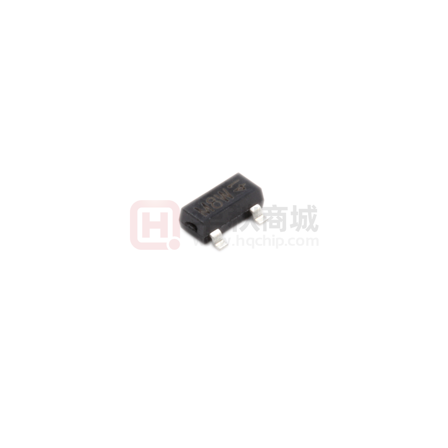
SOT23
D
• Power management functions
• DC-DC Converters
• Backlighting
G
S
Top View
■
MAXIMUM RATINGS
Characteristic
Symbol
Unit
Max
50
V
V GS
+ 20
V
Drain Current- continuous
IDR
173
mA
Drain Current-pulsed
IDRM
700
mA
Drain-Source Voltage
BVDSS
Gate- Source Voltage
■ THERMAL CHARACTERISTICS
Characteristic
Total Device Dissipation TA=25℃
Derate above25℃
Thermal Resistance Junction to Ambient
Junction and Storage Temperature
1
Symbol
Max
Unit
PD
830
1 .8
mW
mW/℃
R ΘJA
350
℃/W
T J, Tstg
150℃,-55to+150℃
�BSN20
N-Channel Enhancement-Mode MOSFET
■ ELECTRICAL CHARACTERISTICS
(TA=25℃ unless otherwise noted)
Characteristic
Drain-Source Breakdown Voltage
(ID =10uA, VGS=0V)
Gate Threshold Voltage
(ID =1mA ,VGS= VDS)
Drain-Source On Voltage
(ID=50mA,VGS=5V)
(ID =500mA,VGS=10V)
Diode Forward Voltage Drop
(ISD=180mA, VGS=0V)
Zero Gate Voltage Drain Current
(VGS=0V, VDS= 40V)
(VGS=0V, VDS=40V, TA=150℃)
Gate Body Leakage
(VGS=+20V, VDS=0V)
Static Drain-Source On-State Resistance
(ID=100mA,VGS=10V)
(ID=100mA,VGS=5V)
(ID=10mA,VGS=2.5V)
Input Capacitance
(VGS=0V, VDS=10V,f=1MHz)
Common Source Output Capacitance
Symbol
Min
Typ
Max
Unit
BVDSS
50
—
—
V
VGS(th)
0.4
—
1.8
V
VDS(ON)
—
—
0.375
3.75
V
VSD
—
—
1.5
V
IDSS
—
—
1
10
uA
IGSS
—
—
+100
nA
RDS(ON)
—
—
CISS
—
—
25
pF
COSS
—
—
15
pF
t(on)
—
—
8
ns
t(off)
—
—
15
ns
trr
—
30
—
ns
(VGS=0V, V DS=10V,f=1MHz)
Turn-ON Time
(VDS=20V, VGS=10V, RGEN=50Ω)
Turn-OFF Time
(VDS=20V, VGS=10V, RGEN=50Ω)
Reverse Recovery Time
(ISD=180mA, VGS=0V)
1. FR-5=1.0×0.75×0.062in.
2 . Alumina=0.4×0.3×0.024in.99.5%alumina.
3 . Pulse Width
很抱歉,暂时无法提供与“BSN20”相匹配的价格&库存,您可以联系我们找货
免费人工找货- 国内价格
- 1+0.22750
- 10+0.21450
- 30+0.18850
- 100+0.16900
- 500+0.15600
- 1000+0.14690