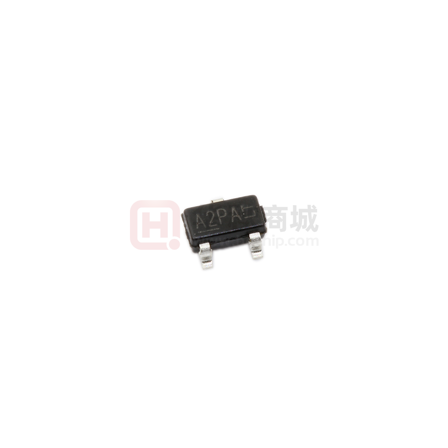
AO3402
N-Channel Enhancement Mode MOSFET
Feature
30V/4.2A
RDS(ON) = 50mΩ(MAX)
@VGS = 10V.
RDS(ON) =60mΩ(MAX)
@VGS = 4.5V.
Super High dense cell design for extremely low RDS(ON) .
Reliable and Rugged.
SC-59 for Surface Mount Package.
SC-59
Applications
●
Power Management
Portable Equipment and Battery Powered Systems.
Absolute Maximum Ratings
Drain-Source Voltage
Gate-Source Voltage
Drain Current-Continuous
Parameter
Electrical Characteristics
Parameter
Off Characteristics
Drain to Source Breakdown Voltage
Zero-Gate Voltage Drain Current
Gate Body Leakage Current, Forward
Gate Body Leakage Current, Reverse
TA=25℃Unless Otherwise noted
Symbol
VDS
VGS
ID
TA=25℃Unless Otherwise noted
Symbol
Test Conditions
Limit
Units
30
±12
4.2
V
V
A
Min
Typ.
Max
Units
-
V
BVDSS
VGS=0V, ID=250μA
30
-
IDSS
VDS=30V, VGS=0V
-
-
1
μA
IGSSF
IGSSR
VGS=12V, VDS=0V
VGS=-12V, VDS=0V
-
-
100
-100
nA
nA
VGS(th)
VGS= VDS, ID=250µA
0.6
-
2.5
V
RDS(ON)
VGS =10V, ID =4A
VGS =4.5V, ID =3A
-
48
55
50
60
mΩ
mΩ
VGS =2.5V, ID =2A
-
60
65
mΩ
1.2
V
On Characteristics
Gate Threshold Voltage
Static Drain-source
On-Resistance
Drain-Source Diode Characteristics and Maximum Ratings
Drain-Source Diode Forward Voltage
VSD
VGS =0V, IS=1.25A
1 of 4
�AO3402
Dynamic
Qg
Qgs
Qgd
ton
td(ON)
tr
Td(off)
tf
toff
Total Gate Charge
Gate-Source Charge
Gate-Drain Charge
Turn-on Time
Turn-on Delay time
Turn-on Rise Time
Turn-off Delay Time
Turn-off Fall Time
Turn-off Time
VDS=15V,VGS=10V,ID=2A
VDD=15V,ID=2A,VGS=10V,RG=6Ω
8.5
1.1
1.8
11
17
37
20
Typical Characteristics
Figure 1.Output Characteristics
Figure 2.Transfer Characteristics
Typical Characteristics
Figure 3.Gate Threshold Variation
with Temperature
Figure 4.On-Resistance Variation
with Temperature
2 of 4
12
nC
40
nS
60
�AO3402
Figure 5.On-Resistance vs. Gate-to-Source
Voltage
Voltage
3 of 4
Figure 6 .Source-Drain Diode Forward
�AO3402
Package Outline Dimensions (UNIT: mm)
4 of 4
�
很抱歉,暂时无法提供与“AO3402”相匹配的价格&库存,您可以联系我们找货
免费人工找货- 国内价格
- 5+0.26565
- 20+0.24090
- 100+0.21615
- 500+0.19140
- 1000+0.17985
- 2000+0.17160
