DW01x-DS-17_EN
May 2014
FO
Fo P R
r R ro TU
ef pe NE
er rti
'
en es
ce
O
nl
y
REV. 1.7
7
Datasheet
DW01x
One Cell Lithium-ion/Polymer Battery Protection IC
�DW01x
Fortune Semiconductor Corporation
富晶電子股份有限公司
23F., No.29-5,Sec. 2, Zhongzheng E. Rd.,
FO
Fo P R
r R ro TU
ef pe NE
er rti
'
en es
ce
O
nl
y
Danshui Dist, New Taipei City 251, Taiwan
Tel.:886-2-28094742
Fax:886-2-28094874
www.ic-fortune.com
This manual contains new product information. Fortune Semiconductor Corporation reserves the
rights to modify the product specification without further notice. No liability is assumed by Fortune
Semiconductor Corporation as a result of the use of this product. No rights under any patent
accompany the sale of the product.
Rev. 1.7
2/19
�DW01x
1.
General Description
Ordering Information
DW01x-x
Serial code form G
Serial code form - & +
Serial code from A to C&E、F *
PACKAGE TYPE
SOT-23-6 (Green-Package)
Refer to the product name list on the next page
FO
Fo P R
r R ro TU
ef pe NE
er rti
'
en es
ce
O
nl
y
The DW01 series battery protection IC is designed
to protect lithium-ion/polymer battery from damage
or degrading the lifetime due to overcharge,
overdischarge, and/or overcurrent for one-cell
lithium-ion/polymer battery powered systems, such
as cellular phones.
The ultra-small package and less required external
components make it ideal to integrate the DW01
series into the limited space of battery pack. The
accurate ±50mV overcharging detection voltage
ensures safe and full utilization charging. The very
low standby current drains little current from the cell
while in storage.
3.
2.
4.
z
Applications
Protection IC for One-Cell Lithium-Ion /
Lithium-Polymer Battery Pack
Features
z
Reduction in Board Size due to Miniature
Package SOT-23-6.
z
Ultra-Low Quiescent Current at 3μA
(Vcc=3.9V).
z
Ultra-Low Power-Down Current at 0.1μA or
Overdischarge Current at 3.5μA (Vcc=2.0V).
z
Precision Overcharge Protection Voltage
4.25V~4.35, accuracy of ± 50mV.
z
0V battery change function are selectable.
z
Power-down fuction are selectable.
z
Load Detection Function during
Overcharge Mode.
z
Two Detection Levels for Overcurrent
Protection.
z
Delay times are generated by internal
circuits. No external capacitors required.
Rev. 1.7
3/19
�DW01x
5.
Product Name List
Model
Overcharge Overcharge Overdischarge Overdischarge Overcurrent
detection
release
detection
release
detection
0V Stand by
voltage
voltage
voltage
voltage
voltage
charge function
Package
[VOI1]
[VODR]
[VODP]
[VOCR]
[VOCP]
function release
(V)
(V)
(mV)
DW01+G SOT-23-6 4.300±0.050 4.100±0.050
2.40±0.100
3.0±0.100
150±30
NO
-
DW01-G SOT-23-6 4.250±0.050 4.050±0.050
2.40±0.100
3.0±0.100
150±30
NO
-
DW01A-G SOT-23-6 4.300±0.050 4.100±0.050
2.40±0.100
3.0±0.100
150±30
NO
AUTO
recovery
DW01B-G SOT-23-6 4.300±0.050 4.100±0.050
2.40±0.100
3.0±0.100
150±30
YES
-
2.980±0.100
150±30
NO
AUTO
recovery
(V)
FO
Fo P R
r R ro TU
ef pe NE
er rti
'
en es
ce
O
nl
y
(V)
DW01C-G SOT-23-6 4.250±0.050 4.050±0.050 2.380±0.100
DW01E-G SOT-23-6 4.280±0.050 4.080±0.050
2.40±0.100
3.0±0.100
150±30
NO
AUTO
recovery
DW01F-G SOT-23-6 4.350±0.050 4.150±0.050
2.40±0.100
3.0±0.100
150±30
NO
AUTO
recovery
6.
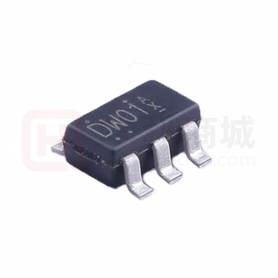
Pin Configuration and Package Marking Information
Pin No.
Symbol
Description
1
OD
MOSFET gate connection pin for discharge control
2
CS
Input pin for current sense, charger detect
3
OC
MOSFET gate connection pin for charge control
4
TD
Test pin for reduce delay time
5
VCC
Power supply, through a resistor (R1)
6
GND
Ground pin
For DW01A~C & E、F
X instead of series code A ~C & E、F
Top Point:Lot No
Bottom Point:Year
w : week, A~Z & A ~ Z
Rev. 1.7
For DW01+、DW01Top Point:Lot No
Bottom Point:Year
w : week, A~Z & A ~ Z
4/19
�DW01x
Functional Block Diagram
TD
7.
VCC
Short circuit
Detector
VSS
VSS
Oscillator
Control
Circuit
Overcharge
Detector
FO
Fo P R
r R ro TU
ef pe NE
er rti
'
en es
ce
O
nl
y
Over current
Detector
Overdischarg
e Detector
CS
Charger
Detector
GND
VSS
OD
OC
Control
Logic
GND
8.
VSS
Divider
Control
Logic
Typical Application Circuit
Symbol
R1
Purpose
ESD protection.
For power fluctuation.
Recommended
470Ω
C1
R2
For power fluctuation.
Protection for reverse
connection of a
charger.
0.1μF
1k~2kΩ
Rev. 1.7
Remakes
Resistance should be as small as
possible to avoid lowering of the
overcharge detection accuracy
caused by VDD pin current. Use
470Ω for better ESD protection.
Select a resistance as large as
possible to prevent large current
when a charge is connected in
reverse.
5/19
�DW01x
9.
Absolute Maximum Ratings
(GND=0V, Ta=25°C unless otherwise specified)
Symbol
Rating
Unit
Input voltage between VCC and GND *
VCC
GND-0.3 to GND+10
V
OC output pin voltage
VOC
VCC -24 to VCC +0.3
V
OD output pin voltage
VOD
GND-0.3 to VCC +0.3
V
CS input pin voltage
VCS
VCC -24 to VCC +0.3
V
FO
Fo P R
r R ro TU
ef pe NE
er rti
'
en es
ce
O
nl
y
Item
Operating Temperature Range
TOP
-40 to +85
°C
Storage Temperature Range
TST
-40 to +125
°C
Note: DW01series contains a circuit that will protect it from static discharge; but please take special care that
no excessive static electricity or voltage which exceeds the limit of the protection circuit will be applied
to it.
Rev. 1.7
6/19
�DW01x
10. Electrical Characteristics
(Ta=25°C unless otherwise specified)
1. DW01+G
TEST CONDITIONS SYMBOL
Min
Typ
Max
UNIT
Supply Current
VCC=3.9V
ICC
3.0
6.0
μA
Power-Down Current
VCC=2.0V
IPD
0.1
μA
Overcharge Protection Voltage
DW01+
VOCP
4.25
4.30
4.35
V
Overcharge Release Voltage
VOCR
4.05
4.10
4.15
V
Overdischarge Protection Voltage
VODP
2.30
2.40
2.50
V
Overdischarge Release Voltage
VODR
2.90
3.00
3.10
V
Overcurrent Protection Voltage
VOIP
(VOI1)
120
150
180
mV
VSIP
(VOI2)
1.00
1.35
1.70
V
1.5
V
FO
Fo P R
r R ro TU
ef pe NE
er rti
'
en es
ce
O
nl
y
PARAMETER
Short Current Protection Voltage
VCC=3.6V
0V Battery Charge Inhibition Battery 0V Battery Charging
Voltage
Unavailable
V0INH
Overcharge Delay Time
TOC
80
200
ms
Overdischarge Delay Time
VCC=3.6V to 2.0V
TOD
40
100
ms
Overcurrent Delay Time (1)
VCC=3.6V
TOI1
10
20
ms
Overcurrent Delay Time (2)
VCC=3.6V
TOI2
5
50
μs
-0.7
-0.2
V
Charger Detection Threshold
Voltage
VCHA
-1.2
OD Pin Output “H” Voltage
VDH
VCC-0.1 VCC-0.02
OD Pin Output “L” Voltage
VDL
OC Pin Output “H” Voltage
VCH
OC Pin Output “L” Voltage
VCL
Rev. 1.7
0. 1
V
0.5
VCC-0.1 VCC-0.02
0.1
V
V
0.5
V
7/19
�DW01x
(2)DW01-G
TEST CONDITIONS SYMBOL
Min
Typ
Max
UNIT
Supply Current
VCC=3.9V
ICC
3.0
6.0
μA
Power-Down Current
VCC=2.0V
IPD
0.1
μA
Overcharge Protection Voltage
DW01-
VOCP
4.20
4.25
4.30
V
Overcharge Release Voltage
VOCR
4.00
4.05
4.10
V
Overdischarge Protection Voltage
VODP
2.30
2.40
2.50
V
Overdischarge Release Voltage
VODR
2.90
3.00
3.10
V
Overcurrent Protection Voltage
VOIP
(VOI1)
120
150
180
mV
VSIP
(VOI2)
1.00
1.35
1.70
V
1.5
V
FO
Fo P R
r R ro TU
ef pe NE
er rti
'
en es
ce
O
nl
y
PARAMETER
Short Current Protection Voltage
VCC=3.6V
0V Battery Charge Inhibition Battery 0V Battery Charging
Voltage
Unavailable
V0INH
Overcharge Delay Time
TOC
80
200
ms
Overdischarge Delay Time
VCC=3.6V to 2.0V
TOD
40
100
ms
Overcurrent Delay Time (1)
VCC=3.6V
TOI1
10
20
ms
Overcurrent Delay Time (2)
VCC=3.6V
TOI2
5
50
μs
-0.7
-0.2
V
Charger Detection Threshold
Voltage
VCHA
-1.2
OD Pin Output “H” Voltage
VDH
VCC-0.1 VCC-0.02
OD Pin Output “L” Voltage
VDL
OC Pin Output “H” Voltage
VCH
OC Pin Output “L” Voltage
VCL
Rev. 1.7
0. 1
V
0.5
VCC-0.1 VCC-0.02
0.1
V
V
0.5
V
8/19
�DW01x
(3)DW01A-G
TEST CONDITIONS SYMBOL
Supply Current
VCC=3.9V
Overdischarge Current
Overcharge Protection Voltage
Min
Typ
Max
UNIT
ICC
3.0
6.0
μA
VCC=2.0V
IOD
1.5
3.5
μA
DW01A
VOCP
4.25
4.30
4.35
V
Overcharge Release Voltage
VOCR
4.05
4.10
4.15
V
Overdischarge Protection Voltage
VODP
2.30
2.40
2.50
V
Overdischarge Release Voltage
VODR
2.90
3.00
3.10
V
Overcurrent Protection Voltage
VOIP
(VOI1)
120
150
180
mV
VSIP
(VOI2)
1.00
1.35
1.70
V
1.5
V
FO
Fo P R
r R ro TU
ef pe NE
er rti
'
en es
ce
O
nl
y
PARAMETER
Short Current Protection Voltage
VCC=3.6V
0V Battery Charge Inhibition Battery 0V Battery Charging
Voltage
Unavailable
V0INH
Overcharge Delay Time
TOC
80
200
ms
Overdischarge Delay Time
VCC=3.6V to 2.0V
TOD
40
100
ms
Overcurrent Delay Time (1)
VCC=3.6V
TOI1
10
20
ms
Overcurrent Delay Time (2)
VCC=3.6V
TOI2
5
50
μs
-0.7
-0.2
V
Charger Detection Threshold
Voltage
VCHA
-1.2
OD Pin Output “H” Voltage
VDH
VCC-0.1 VCC-0.02
OD Pin Output “L” Voltage
VDL
OC Pin Output “H” Voltage
VCH
OC Pin Output “L” Voltage
VCL
Rev. 1.7
0. 1
V
0.5
VCC-0.1 VCC-0.02
0.1
V
V
0.5
V
9/19
�DW01x
(4)DW01B-G
TEST CONDITIONS
SYMBOL Min
Typ
Max
UNIT
Supply Current
VCC=3.9V
ICC
3.0
6.0
μA
Power-Down Current
VCC=2.0V
IPD
0.1
μA
Overcharge Protection Voltage
DW01B
VOCP
4.25
4.30
4.35
V
Overcharge Release Voltage
VOCR
4.05
4.10
4.15
V
Overdischarge Protection Voltage
VODP
2.30
2.40
2.50
V
Overdischarge Release Voltage
VODR
2.90
3.00
3.10
V
Overcurrent Protection Voltage
VOIP
120
(VOI1)
150
180
mV
VSIP
1.00
(VOI2)
1.35
1.70
V
FO
Fo P R
r R ro TU
ef pe NE
er rti
'
en es
ce
O
nl
y
PARAMETER
Short Current Protection Voltage
VCC=3.6V
0V Battery Charger Starting Charge 0V Battery Charging
Voltage
Available
V0CHA
Overcharge Delay Time
TOC
80
200
ms
1.5
V
Overdischarge Delay Time
VCC=3.6V to 2.0V
TOD
40
100
ms
Overcurrent Delay Time (1)
VCC=3.6V
TOI1
10
20
ms
Overcurrent Delay Time (2)
VCC=3.6V
TOI2
5
50
μs
-0.7
-0.2
V
Charger Detection Threshold
Voltage
VCHA
-1.2
OD Pin Output “H” Voltage
VDH
VCC-0.1 VCC-0.02
OD Pin Output “L” Voltage
VDL
OC Pin Output “H” Voltage
VCH
OC Pin Output “L” Voltage
VCL
0. 1
V
0.5
VCC-0.1 VCC-0.02
0.1
V
V
0.5
V
Note: The V0CHA is defined as the voltage between VCC and VCS (VCC-VCS>1.5V) at which OC
pin goes “H” when the voltage VCC is gradually increased to the VCC=1V and VCS=-0.5V.
Rev. 1.7
10/19
�DW01x
(5)DW01C-G
TEST CONDITIONS SYMBOL
Supply Current
VCC=3.9V
Overdischarge Current
Overcharge Protection Voltage
Min
Typ
Max
UNIT
ICC
3.0
6.0
μA
VCC=2.0V
IOD
1.5
3.5
μA
DW01C
VOCP
4.25
4.30
V
4.20
FO
Fo P R
r R ro TU
ef pe NE
er rti
'
en es
ce
O
nl
y
PARAMETER
Overcharge Release Voltage
VOCR
4.00
4.05
4.10
V
Overdischarge Protection Voltage
VODP
2.28
2.38
2.48
V
Overdischarge Release Voltage
VODR
2.880
2.980
3.080
V
Overcurrent Protection Voltage
VOIP
(VOI1)
120
150
180
mV
VSIP
(VOI2)
1.00
1.35
1.70
V
1.5
V
Short Current Protection Voltage
VCC=3.6V
0V Battery Charge Inhibition Battery 0V Battery Charging
Voltage
Unavailable
V0INH
Overcharge Delay Time
TOC
80
200
ms
Overdischarge Delay Time
VCC=3.6V to 2.0V
TOD
40
100
ms
Overcurrent Delay Time (1)
VCC=3.6V
TOI1
10
20
ms
Overcurrent Delay Time (2)
VCC=3.6V
TOI2
5
50
μs
-0.7
-0.2
V
Charger Detection Threshold
Voltage
VCHA
-1.2
OD Pin Output “H” Voltage
VDH
VCC-0.1 VCC-0.02
OD Pin Output “L” Voltage
VDL
OC Pin Output “H” Voltage
VCH
OC Pin Output “L” Voltage
VCL
Rev. 1.7
0. 1
V
0.5
VCC-0.1 VCC-0.02
0.1
V
V
0.5
V
11/19
�DW01x
(6)DW01E-G
TEST CONDITIONS SYMBOL
Supply Current
VCC=3.9V
Overdischarge Current
Overcharge Protection Voltage
Min
Typ
Max
UNIT
ICC
3.0
6.0
μA
VCC=2.0V
IOD
1.5
3.5
μA
DW01E
VOCP
4.28
4.33
V
4.23
FO
Fo P R
r R ro TU
ef pe NE
er rti
'
en es
ce
O
nl
y
PARAMETER
Overcharge Release Voltage
VOCR
4.03
4.08
4.13
V
Overdischarge Protection Voltage
VODP
2.30
2.40
2.50
V
Overdischarge Release Voltage
VODR
2.90
3.00
3.10
V
Overcurrent Protection Voltage
VOIP
(VOI1)
120
150
180
mV
VSIP
(VOI2)
1.00
1.35
1.70
V
1.5
V
Short Current Protection Voltage
VCC=3.6V
0V Battery Charge Inhibition Battery 0V Battery Charging
Voltage
Unavailable
V0INH
Overcharge Delay Time
TOC
80
200
ms
Overdischarge Delay Time
VCC=3.6V to 2.0V
TOD
40
100
ms
Overcurrent Delay Time (1)
VCC=3.6V
TOI1
10
20
ms
Overcurrent Delay Time (2)
VCC=3.6V
TOI2
5
50
μs
-0.7
-0.2
V
Charger Detection Threshold
Voltage
VCHA
-1.2
OD Pin Output “H” Voltage
VDH
VCC-0.1 VCC-0.02
OD Pin Output “L” Voltage
VDL
OC Pin Output “H” Voltage
VCH
OC Pin Output “L” Voltage
VCL
Rev. 1.7
0. 1
V
0.5
VCC-0.1 VCC-0.02
0.1
V
V
0.5
V
12/19
�DW01x
(7)DW01F-G
TEST CONDITIONS SYMBOL
Supply Current
VCC=3.9V
Overdischarge Current
Overcharge Protection Voltage
Min
Typ
Max
UNIT
ICC
3.0
6.0
μA
VCC=2.0V
IOD
1.5
3.5
μA
DW01F
VOCP
4.30
4.35
4.40
V
Overcharge Release Voltage
VOCR
4.10
4.15
4.20
V
Overdischarge Protection Voltage
VODP
2.30
2.40
2.50
V
Overdischarge Release Voltage
VODR
2.90
3.00
3.10
V
Overcurrent Protection Voltage
VOIP
(VOI1)
120
150
180
mV
VSIP
(VOI2)
1.00
1.35
1.70
V
1.5
V
FO
Fo P R
r R ro TU
ef pe NE
er rti
'
en es
ce
O
nl
y
PARAMETER
Short Current Protection Voltage
VCC=3.6V
0V Battery Charge Inhibition Battery 0V Battery Charging
Voltage
Unavailable
V0INH
Overcharge Delay Time
TOC
80
200
ms
Overdischarge Delay Time
VCC=3.6V to 2.0V
TOD
40
100
ms
Overcurrent Delay Time (1)
VCC=3.6V
TOI1
10
20
ms
Overcurrent Delay Time (2)
VCC=3.6V
TOI2
5
50
μs
-0.7
-0.2
V
Charger Detection Threshold
Voltage
VCHA
-1.2
OD Pin Output “H” Voltage
VDH
VCC-0.1 VCC-0.02
OD Pin Output “L” Voltage
VDL
OC Pin Output “H” Voltage
VCH
OC Pin Output “L” Voltage
VCL
Rev. 1.7
0. 1
V
0.5
VCC-0.1 VCC-0.02
0.1
V
V
0.5
V
13/19
�DW01x
11. Description of Operation
Normal Condition
If VODP
很抱歉,暂时无法提供与“DW01A-G”相匹配的价格&库存,您可以联系我们找货
免费人工找货- 国内价格
- 5+0.82603
- 20+0.75315
- 100+0.68026
- 500+0.60737
- 1000+0.57336
- 2000+0.54907