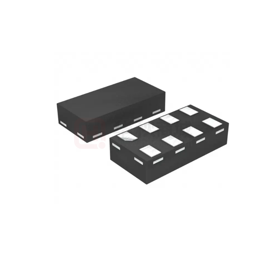
74AVC1T8128
Single dual-supply translating 2-input NOR with enable
Rev. 1 — 10 October 2018
Product data sheet
1. General description
The 74AVC1T8128 is a single dual-supply translating 2-input NOR with enable input. It features
two data input pins (A, B), one enable input pin (E), one data output pin (Y) and dual-supply pins
(VCC(A) and VCC(B)). Both VCC(A) and VCC(B) can be supplied at any voltage between 0.8 V and
3.6 V making the device suitable for translating between any of the low voltage nodes (0.8 V, 1.2 V,
1.5 V, 1.8 V, 2.5 V and 3.3 V). Pins A, B and E are referenced to VCC(A) and pin Y is referenced to
VCC(B).
The logic equation provided at the Y output is:
Y = E + A•B
The device is fully specified for partial power-down applications using IOFF. The IOFF circuitry
disables the output, preventing any damaging backflow current through the device when it is
powered down. In Suspend mode when either VCC(A) or VCC(B) are at GND level, the Y output is in
the high-impedance OFF-state.
2. Features and benefits
•
•
•
•
•
•
•
•
•
•
•
Wide supply voltage range:
• VCC(A): 0.8 V to 3.6 V
• VCC(B): 0.8 V to 3.6 V
High noise immunity
Complies with JEDEC standards:
• JESD8-12 (0.8 V to 1.3 V)
• JESD8-11 (0.9 V to 1.65 V)
• JESD8-7 (1.2 V to 1.95 V)
• JESD8-5 (1.8 V to 2.7 V)
• JESD8-B (2.7 V to 3.6 V)
ESD protection:
• HBM: ANSI/ESDA/JEDEC JS-001 exceeds 8000 V
• CDM: ANSI/ESDA/JEDEC JS-002 exceeds 1000 V
Maximum data rates:
• 500 Mbit/s (1.8 V to 3.3 V translation)
• 320 Mbit/s (
很抱歉,暂时无法提供与“74AVC1T8128GSX”相匹配的价格&库存,您可以联系我们找货
免费人工找货