GAN063-650WSA
650 V, 50 mΩ Gallium Nitride (GaN) FET
27 November 2019
Product data sheet
1. General description
The GAN063-650WSA is a 650 V, 50 mΩ Gallium Nitride (GaN) FET. It is a normally-off device that
combines Nexperia’s state-of-the-art high-voltage GaN HEMT and low-voltage silicon MOSFET
technologies — offering superior reliability and performance. AEC-Q101 qualified.
2. Features and benefits
•
•
•
•
•
•
•
Ultra-low reverse recovery charge
Simple gate drive (0 V to +10 V or 12 V)
Robust gate oxide (±20 V capability)
High gate threshold voltage (+4 V) for very good gate bounce immunity
Very low source-drain voltage in reverse conduction mode
Transient over-voltage capability (800 V)
AEC-Q101 qualified
3. Applications
•
•
•
•
Hard and soft switching converters for industrial and datacom power
Bridgeless totempole PFC
PV and UPS inverters
Servo motor drives
4. Quick reference data
Table 1. Quick reference data
Symbol
Parameter
Conditions
Min
Typ
Max
Unit
VDS
drain-source voltage
-55 °C ≤ Tj ≤ 175 °C
-
-
650
V
ID
drain current
VGS = 10 V; Tmb = 25 °C; Fig. 2
-
-
34.5
A
Ptot
total power dissipation
Tmb = 25 °C; Fig. 1
-
-
143
W
Tj
junction temperature
-55
-
175
°C
VGS = 10 V; ID = 25 A; Tj = 25 °C
-
50
60
mΩ
ID = 25 A; VDS = 400 V; VGS = 10 V;
Tj = 25 °C
-
4
-
nC
-
15
-
nC
IS = 25 A; dIS/dt = -1000 A/µs;
VGS = 0 V; VDS = 400 V; Fig. 14
-
125
-
nC
Static characteristics
RDSon
drain-source on-state
resistance
Dynamic characteristics
QGD
gate-drain charge
QG(tot)
total gate charge
Source-drain diode
Qr
recovered charge
�GAN063-650WSA
Nexperia
650 V, 50 mΩ Gallium Nitride (GaN) FET
5. Pinning information
Table 2. Pinning information
Pin
Symbol
Description
Simplified outline
1
G
gate
2
S
source
3
D
drain
mb
S
mounting base; connected
to source
Graphic symbol
mb
D
G
1
2
S
3
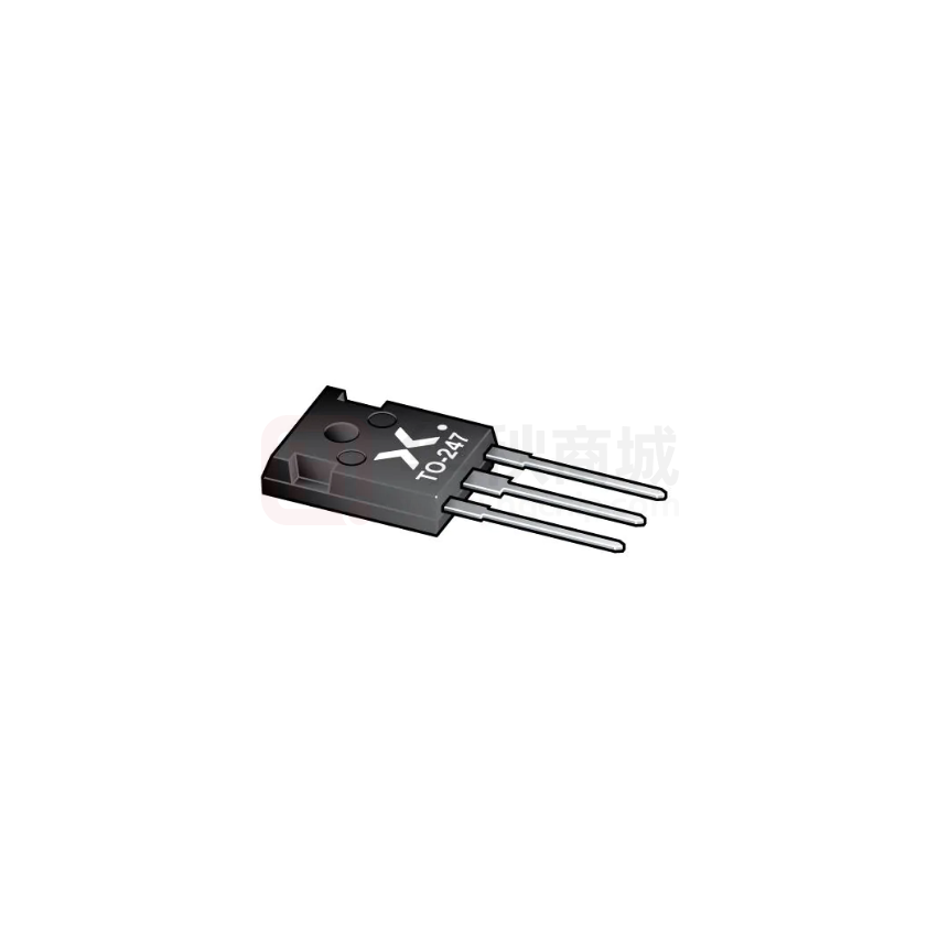
TO-247 (SOT429)
aaa-028116
6. Ordering information
Table 3. Ordering information
Type number
Package
GAN063-650WSA
Name
Description
Version
TO-247
plastic, single-ended through-hole package; 3 leads; 5.45 mm
pitch; 20.45 mm x 15.6 mm x 4.95 mm body
SOT429
7. Marking
Table 4. Marking codes
Type number
Marking code
GAN063-650WSA
GAN063-650WSA
GAN063-650WSA
Product data sheet
All information provided in this document is subject to legal disclaimers.
27 November 2019
©
Nexperia B.V. 2019. All rights reserved
2 / 12
�GAN063-650WSA
Nexperia
650 V, 50 mΩ Gallium Nitride (GaN) FET
8. Limiting values
Table 5. Limiting values
In accordance with the Absolute Maximum Rating System (IEC 60134).
Symbol
Parameter
Conditions
Min
Max
Unit
VDS
drain-source voltage
-55 °C ≤ Tj ≤ 175 °C
-
650
V
VTDS
transient drain to source
voltage
pulsed; tp = 1 µs; δfactor = 0.01
-
800
V
VGS
gate-source voltage
-20
20
V
Ptot
total power dissipation
Tmb = 25 °C; Fig. 1
-
143
W
ID
drain current
VGS = 10 V; Tmb = 25 °C; Fig. 2
-
34.5
A
VGS = 10 V; Tmb = 100 °C; Fig. 2
-
24.4
A
pulsed; tp ≤ 10 µs; Tmb = 25 °C; Fig. 3
IDM
peak drain current
-
150
A
Tstg
storage temperature
-55
175
°C
Tj
junction temperature
-55
175
°C
Tsld(M)
peak soldering
temperature
-
260
°C
Source-drain diode
IS
source current
Tmb = 25 °C; VGS = 0 V
-
34.5
A
ISM
peak source current
pulsed; tp ≤ 10 µs; Tmb = 25 °C
-
150
A
03aa16
120
Pder
(%)
aaa-028050
100
ID
(A)
D = 10%
80
D = 20%
80
60
D = 50%
40
40
DC
20
0
0
50
100
150
Tmb (°C)
0
200
25
50
75
100
125
150
175
Tmb (°C)
200
VGS ≥ 10 V; Pulse width ≤ 10 µs
Fig. 2.
Fig. 1.
Normalized total power dissipation as a
function of mounting base temperature
GAN063-650WSA
Product data sheet
Drain current as a function of mounting base
temperature
All information provided in this document is subject to legal disclaimers.
27 November 2019
©
Nexperia B.V. 2019. All rights reserved
3 / 12
�GAN063-650WSA
Nexperia
650 V, 50 mΩ Gallium Nitride (GaN) FET
ID
(A)
aaa-028052
103
tp = 1 µs
102
100 µs
10
10 µs
1 ms
10 ms
1
10-1
10-2
10-1
1
102
10
103
VDS (V)
Tmb = 25 °C; IDM is a single pulse
Fig. 3.
Safe operating area; continuous and peak drain currents as a function of drain-source voltage
9. Thermal characteristics
Table 6. Thermal characteristics
Symbol
Parameter
Min
Typ
Max
Unit
Rth(j-mb)
thermal resistance from Fig. 4
junction to mounting
base
Conditions
-
-
1.05
K/W
Rth(j-a)
thermal resistance from vertical in free air
junction to ambient
-
-
40
K/W
aaa-028054
10
Zth(j-mb)
(K/W)
1 δ = 0.5
0.2
10-1
0.1
10-2
P
single shot
δ=
Fig. 4.
10-5
10-4
10-3
10-2
T
t
tp
10-3
10-6
tp
T
10-1
tp (s)
1
Transient thermal impedance from junction to mounting base as a function of pulse duration
GAN063-650WSA
Product data sheet
All information provided in this document is subject to legal disclaimers.
27 November 2019
©
Nexperia B.V. 2019. All rights reserved
4 / 12
�GAN063-650WSA
Nexperia
650 V, 50 mΩ Gallium Nitride (GaN) FET
10. Characteristics
Table 7. Characteristics
Symbol
Parameter
Conditions
Min
Typ
Max
Unit
ID = 1 mA; VDS=VGS; Tj = 25 °C
3.4
3.9
4.5
V
ID = 1 mA; VDS=VGS; Tj = 175 °C; Fig. 9
2.2
-
-
V
ID = 1 mA; VDS=VGS; Tj = -55 °C; Fig. 9
-
-
5.2
V
VDS = 650 V; VGS = 0 V; Tj = 25 °C
-
2
25
µA
VDS = 650 V; VGS = 0 V; Tj = 175 °C
-
25
-
µA
VGS = -20 V; VDS = 0 V; Tj = 25 °C
-
10
100
nA
VGS = 20 V; VDS = 0 V; Tj = 25 °C
-
10
100
nA
drain-source on-state
resistance
VGS = 10 V; ID = 25 A; Tj = 25 °C
-
50
60
mΩ
VGS = 10 V; ID = 25 A; Tj = 175 °C;
Fig. 10
-
120
-
mΩ
gate resistance
f = 1 MHz
-
2.3
-
Ω
ID = 25 A; VDS = 400 V; VGS = 10 V;
Tj = 25 °C
-
15
-
nC
-
6
-
nC
-
4
-
nC
-
1000
-
pF
-
130
-
pF
-
8
-
pF
Static characteristics
VGS(th)
IDSS
IGSS
RDSon
RG
gate-source threshold
voltage
drain leakage current
gate leakage current
Dynamic characteristics
QG(tot)
total gate charge
QGS
gate-source charge
QGD
gate-drain charge
Ciss
input capacitance
Coss
output capacitance
Crss
reverse transfer
capacitance
Co(er)
effective output
capacitance, energy
related
0 V ≤ VDS ≤ 400 V; VGS = 0 V;
Tj = 25 °C; Fig. 12
-
190
-
pF
Co(tr)
effective output
capacitance, time
related
0 V ≤ VDS ≤ 400 V; VGS = 0 V;
Tj = 25 °C
-
310
-
pF
td(on)
turn-on delay time
-
57
-
ns
tr
rise time
VDS = 400 V; RL = 16 Ω; VGS = 12 V;
RG(ext) = 40 Ω
-
10
-
ns
td(off)
turn-off delay time
-
88
-
ns
tf
fall time
-
11
-
ns
Qoss
output charge
VGS = 0 V; VDS = 400 V
-
125
-
nC
IS = 25 A; VGS = 0 V; Tj = 25 °C; Fig. 13
-
1.9
-
V
IS = 12.5 A; VGS = 0 V; Tj = 25 °C
-
1.35
-
V
IS = 25 A; dIS/dt = -1000 A/µs;
VGS = 0 V; VDS = 400 V; Fig. 14
-
54
-
ns
-
125
-
nC
VDS = 400 V; VGS = 0 V; f = 1 MHz;
Tj = 25 °C; Fig. 11
Source-drain diode
VSD
source-drain voltage
trr
reverse recovery time
Qr
recovered charge
GAN063-650WSA
Product data sheet
All information provided in this document is subject to legal disclaimers.
27 November 2019
©
Nexperia B.V. 2019. All rights reserved
5 / 12
�GAN063-650WSA
Nexperia
650 V, 50 mΩ Gallium Nitride (GaN) FET
aaa-028060
200
ID
(A)
aaa-028061
100
ID
(A)
VGS = 10 V
VGS = 10 V
80
150
7.5 V
8V
7V
60
7V
100
40
50
0
Fig. 5.
ID
(A)
6V
20
5V
5V
0
2
4
6
8
VDS (V)
0
10
0
2
4
6
8
VDS (V)
10
Tj = 25 °C
Tj = 175 °C
Output characteristics; drain current as a
Fig. 6.
function of drain-source voltage; typical values
Output characteristics; drain current as a
function of drain-source voltage; typical values
aaa-028055
80
60
120
40
80
40
175°C
0
aaa-029173
160
QOSS
(nC)
20
0
2
4
Tj = 25°C
6
8
VGS (V)
0
10
VDS = 10 V
Fig. 7.
6V
Transfer characteristics; drain current as a
function of gate-source voltage; typical values
GAN063-650WSA
Product data sheet
Fig. 8.
0
100
300
400
500
600
VDS (V)
700
Typical QOSS
All information provided in this document is subject to legal disclaimers.
27 November 2019
200
©
Nexperia B.V. 2019. All rights reserved
6 / 12
�GAN063-650WSA
Nexperia
650 V, 50 mΩ Gallium Nitride (GaN) FET
VGS(th)
(V)
aaa-029174
6
5
aaa-027810
3
a
2.5
Max
4
2
Typ
3
1.5
Min
2
1
1
0.5
0
-60
-30
0
30
60
90
120 150
Tj (°C)
0
-60
180
-30
0
30
60
90
120 150
Tj (°C)
180
ID = 1 mA ; VDS = VGS
Fig. 9.
Gate-source threshold voltage as a function of
junction temperature
aaa-028058
104
aaa-028063
30
C
(pF)
EOSS
(µJ)
25
Ciss
103
Fig. 10. Normalized drain-source on-state resistance
factor as a function of junction temperature
20
102
15
Coss
10
10
5
Crss
1
1
10
102
VDS (V)
0
103
VGS = 0 V; f = 1 MHz
Fig. 11. Input, output and reverse transfer capacitances
as a function of drain-source voltage; typical
values
GAN063-650WSA
Product data sheet
0
100
200
300
400
500
VDS (V)
600
Fig. 12. Typical COSS Stored Energy
All information provided in this document is subject to legal disclaimers.
27 November 2019
©
Nexperia B.V. 2019. All rights reserved
7 / 12
�GAN063-650WSA
Nexperia
650 V, 50 mΩ Gallium Nitride (GaN) FET
aaa-028059
150
IS
(A)
125
Tj = 25°C
50°C
75°C
100°C
100
125°C
150°C
75
175°C
50
25
0
0
2
4
6
8
VSD (V)
10
VGS = 0 V
Fig. 13. Source-drain (diode forward) current as a function of source-drain (diode forward) voltage; typical values
I, V
dlS/dt
IS
trr
IRM
DUT
A
Qr
0.25 IRM
t
VRRM
VSD
+
aaa-029277
Fig. 14. Diode reverse recovery test circuit and waveform
GAN063-650WSA
Product data sheet
All information provided in this document is subject to legal disclaimers.
27 November 2019
©
Nexperia B.V. 2019. All rights reserved
8 / 12
�GAN063-650WSA
Nexperia
650 V, 50 mΩ Gallium Nitride (GaN) FET
11. Application information
To achieve maximum efficiency and stability when switching high currents, a switching node RC
snubber (Rsn, Csn) is recommended. For IL < 14 A, a switching-node snubber is not required.
CSN is taken from the graph.
RSN should be selected to achieve a time constant of 1 ns; e.g. if CSN = 100 pF,
RSN = 1 ns / 100 pF = 10 Ω.
VBUS
DC bus
aaa-029603
Csn 180
(pF)
160
driver
RG
RCDCL
(place as close as
possible to drain pin)
Q2
140
120
VS
100
driver
RG
Vo
Q1
80
RSN
RCSN
C SN
60
aaa-029331
40
Fig. 16. DC-link snubber circuit
20
0
0
5
10
15
20
25
30
35
IL (A)
40
RG = 30 Ω; τ = RSN × CSN = 1 ns
Fig. 15. Snubber capacitance as function of load current
Note: A DC-link snubber is recommended in all cases. Optimal is 20 nF in series with
4 Ω, most easily achieved with parallel combination 10 nF and 8 Ω. This snubber lowers
the Q factor of any resonance in the bus. That resonance will act as a load on the high
gain amplifier that is the GaN FET and can lead to instability. For very high current, an RC
snubber is recommended for the switching node. This will increase switching loss, so this
is only recommended at high power levels where the losses are a very small percentage of
the total power.
GAN063-650WSA
Product data sheet
All information provided in this document is subject to legal disclaimers.
27 November 2019
©
Nexperia B.V. 2019. All rights reserved
9 / 12
�GAN063-650WSA
Nexperia
650 V, 50 mΩ Gallium Nitride (GaN) FET
12. Package outline
Plastic single-ended through-hole package; heatsink mounted; 1 mounting hole; 3-lead TO-247
A
E
SOT429
E1
A2
E2/2
D2
Q
S
E2
ØP
D
D1
ØP1
1
2
3
L1
A1
b2 (2x)
b4
L
b
(3x)
e
(2x)
c
0
20 mm
scale
øP
øP1
Q
S
3.658 7.315 5.740 6.299
3.556 7.061 5.486 6.045
Dimensions (mm are the original dimensions)
Unit
mm
A
A1
A2
b
b2
b4
c
D
D1
D2
E
E1
E2
max 5.156 2.507 2.108 1.397 2.387 3.429 0.889 21.082 17.441 1.321 16.027 14.148 5.225
nom
min 4.902 2.253 1.854 0.991 1.651 2.591 0.381 20.828 17.187 1.067 15.773 13.894 4.318
E2/2
2.613
2.159
e
5.436
L
L1
20.320 4.445
20.066 3.937
sot429_po
Outline
version
SOT429
References
IEC
JEDEC
JEITA
European
projection
Issue date
19-08-19
19-08-20
TO-247
Fig. 17. Package outline TO-247 (SOT429)
GAN063-650WSA
Product data sheet
All information provided in this document is subject to legal disclaimers.
27 November 2019
©
Nexperia B.V. 2019. All rights reserved
10 / 12
�GAN063-650WSA
Nexperia
650 V, 50 mΩ Gallium Nitride (GaN) FET
13. Legal information
injury, death or severe property or environmental damage. Nexperia and its
suppliers accept no liability for inclusion and/or use of Nexperia products in
such equipment or applications and therefore such inclusion and/or use is at
the customer’s own risk.
Data sheet status
Quick reference data — The Quick reference data is an extract of the
product data given in the Limiting values and Characteristics sections of this
document, and as such is not complete, exhaustive or legally binding.
Document status
[1][2]
Product
status [3]
Definition
Objective [short]
data sheet
Development
This document contains data from
the objective specification for
product development.
Preliminary [short]
data sheet
Qualification
This document contains data from
the preliminary specification.
Product [short]
data sheet
Production
This document contains the product
specification.
[1]
[2]
[3]
Please consult the most recently issued document before initiating or
completing a design.
The term 'short data sheet' is explained in section "Definitions".
The product status of device(s) described in this document may have
changed since this document was published and may differ in case of
multiple devices. The latest product status information is available on
the internet at https://www.nexperia.com.
Definitions
Draft — The document is a draft version only. The content is still under
internal review and subject to formal approval, which may result in
modifications or additions. Nexperia does not give any representations or
warranties as to the accuracy or completeness of information included herein
and shall have no liability for the consequences of use of such information.
Short data sheet — A short data sheet is an extract from a full data sheet
with the same product type number(s) and title. A short data sheet is
intended for quick reference only and should not be relied upon to contain
detailed and full information. For detailed and full information see the relevant
full data sheet, which is available on request via the local Nexperia sales
office. In case of any inconsistency or conflict with the short data sheet, the
full data sheet shall prevail.
Product specification — The information and data provided in a Product
data sheet shall define the specification of the product as agreed between
Nexperia and its customer, unless Nexperia and customer have explicitly
agreed otherwise in writing. In no event however, shall an agreement be
valid in which the Nexperia product is deemed to offer functions and qualities
beyond those described in the Product data sheet.
Disclaimers
Limited warranty and liability — Information in this document is believed
to be accurate and reliable. However, Nexperia does not give any
representations or warranties, expressed or implied, as to the accuracy
or completeness of such information and shall have no liability for the
consequences of use of such information. Nexperia takes no responsibility
for the content in this document if provided by an information source outside
of Nexperia.
In no event shall Nexperia be liable for any indirect, incidental, punitive,
special or consequential damages (including - without limitation - lost
profits, lost savings, business interruption, costs related to the removal
or replacement of any products or rework charges) whether or not such
damages are based on tort (including negligence), warranty, breach of
contract or any other legal theory.
Notwithstanding any damages that customer might incur for any reason
whatsoever, Nexperia’s aggregate and cumulative liability towards customer
for the products described herein shall be limited in accordance with the
Terms and conditions of commercial sale of Nexperia.
Right to make changes — Nexperia reserves the right to make changes
to information published in this document, including without limitation
specifications and product descriptions, at any time and without notice. This
document supersedes and replaces all information supplied prior to the
publication hereof.
Suitability for use — Nexperia products are not designed, authorized or
warranted to be suitable for use in life support, life-critical or safety-critical
systems or equipment, nor in applications where failure or malfunction
of an Nexperia product can reasonably be expected to result in personal
GAN063-650WSA
Product data sheet
Applications — Applications that are described herein for any of these
products are for illustrative purposes only. Nexperia makes no representation
or warranty that such applications will be suitable for the specified use
without further testing or modification.
Customers are responsible for the design and operation of their applications
and products using Nexperia products, and Nexperia accepts no liability for
any assistance with applications or customer product design. It is customer’s
sole responsibility to determine whether the Nexperia product is suitable
and fit for the customer’s applications and products planned, as well as
for the planned application and use of customer’s third party customer(s).
Customers should provide appropriate design and operating safeguards to
minimize the risks associated with their applications and products.
Nexperia does not accept any liability related to any default, damage, costs
or problem which is based on any weakness or default in the customer’s
applications or products, or the application or use by customer’s third party
customer(s). Customer is responsible for doing all necessary testing for the
customer’s applications and products using Nexperia products in order to
avoid a default of the applications and the products or of the application or
use by customer’s third party customer(s). Nexperia does not accept any
liability in this respect.
Limiting values — Stress above one or more limiting values (as defined in
the Absolute Maximum Ratings System of IEC 60134) will cause permanent
damage to the device. Limiting values are stress ratings only and (proper)
operation of the device at these or any other conditions above those
given in the Recommended operating conditions section (if present) or the
Characteristics sections of this document is not warranted. Constant or
repeated exposure to limiting values will permanently and irreversibly affect
the quality and reliability of the device.
Terms and conditions of commercial sale — Nexperia products are
sold subject to the general terms and conditions of commercial sale, as
published at http://www.nexperia.com/profile/terms, unless otherwise agreed
in a valid written individual agreement. In case an individual agreement is
concluded only the terms and conditions of the respective agreement shall
apply. Nexperia hereby expressly objects to applying the customer’s general
terms and conditions with regard to the purchase of Nexperia products by
customer.
No offer to sell or license — Nothing in this document may be interpreted
or construed as an offer to sell products that is open for acceptance or the
grant, conveyance or implication of any license under any copyrights, patents
or other industrial or intellectual property rights.
Export control — This document as well as the item(s) described herein
may be subject to export control regulations. Export might require a prior
authorization from competent authorities.
Non-automotive qualified products — Unless this data sheet expressly
states that this specific Nexperia product is automotive qualified, the
product is not suitable for automotive use. It is neither qualified nor tested in
accordance with automotive testing or application requirements. Nexperia
accepts no liability for inclusion and/or use of non-automotive qualified
products in automotive equipment or applications.
In the event that customer uses the product for design-in and use in
automotive applications to automotive specifications and standards,
customer (a) shall use the product without Nexperia’s warranty of the
product for such automotive applications, use and specifications, and (b)
whenever customer uses the product for automotive applications beyond
Nexperia’s specifications such use shall be solely at customer’s own risk,
and (c) customer fully indemnifies Nexperia for any liability, damages or failed
product claims resulting from customer design and use of the product for
automotive applications beyond Nexperia’s standard warranty and Nexperia’s
product specifications.
Translations — A non-English (translated) version of a document is for
reference only. The English version shall prevail in case of any discrepancy
between the translated and English versions.
Trademarks
Notice: All referenced brands, product names, service names and
trademarks are the property of their respective owners.
All information provided in this document is subject to legal disclaimers.
27 November 2019
©
Nexperia B.V. 2019. All rights reserved
11 / 12
�GAN063-650WSA
Nexperia
650 V, 50 mΩ Gallium Nitride (GaN) FET
Contents
1. General description...................................................... 1
2. Features and benefits.................................................. 1
3. Applications.................................................................. 1
4. Quick reference data....................................................1
5. Pinning information......................................................2
6. Ordering information....................................................2
7. Marking.......................................................................... 2
8. Limiting values............................................................. 3
9. Thermal characteristics............................................... 4
10. Characteristics............................................................ 5
11. Application information..............................................9
12. Package outline........................................................ 10
13. Legal information......................................................11
©
Nexperia B.V. 2019. All rights reserved
For more information, please visit: http://www.nexperia.com
For sales office addresses, please send an email to: salesaddresses@nexperia.com
Date of release: 27 November 2019
GAN063-650WSA
Product data sheet
All information provided in this document is subject to legal disclaimers.
27 November 2019
©
Nexperia B.V. 2019. All rights reserved
12 / 12
�