PJM2300NSA
N-Channel MOSFET
Feature
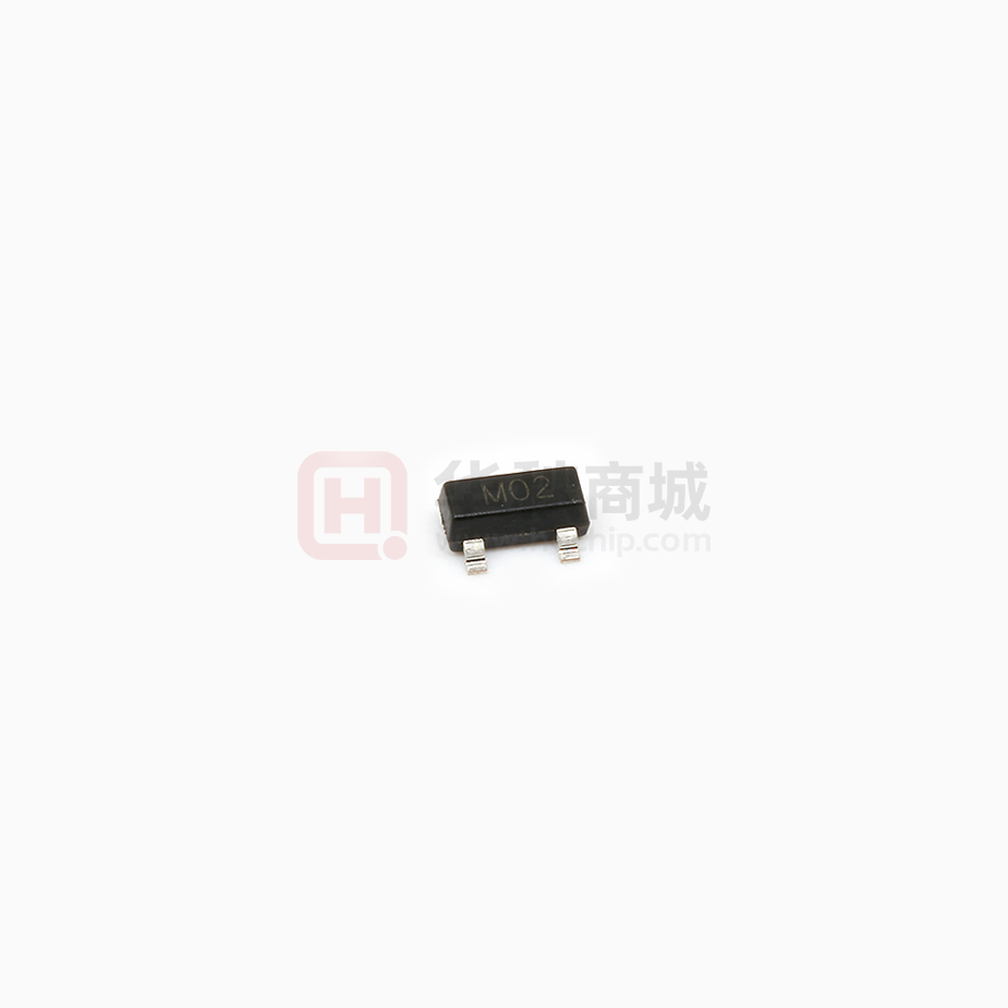
SOT-23
⚫
TrenchFET Power MOSFET
⚫
Excellent RDS(on) and Low Gate Charge
Applications
⚫
Load Switch for Portable Devices
⚫
DC/DC Converter
1. Gate 2.Source 3.Drain
Marking: M02
Schematic diagram
3Drain
1
Gate
2 Source
Absolute Maximum Ratings
Ratings at TA =25℃ unless otherwise specified.
Parameter
Drain-Source Voltage
Symbol
VDS
Maximum
20
Units
V
VGS
±12
V
Continuous Drain Current
ID
4.5
Pulsed Drain Current
IDM
18
PD
0.35
W
TJ, TSTG
150, -55 to 150
°C
Symbol
Typ.
Units
RθJA
357
°C/W
Gate-Source Voltage
A
Note1
Power Dissipation
Junction and Storage Temperature Range
Thermal Characteristics
Parameter
Maximum Junction-to-Ambient
www.pingjingsemi.com
Revision:1.0 Jan-2019
Note2
1/6
�PJM2300NSA
N-Channel MOSFET
Electrical Characteristics (TC = 25℃)
Parameter
Symbol
Conditions
Min.
Typ.
Max.
Units
Static Parameters
Drain-Source Breakdown Voltage
BVDSS
ID=250µA, VGS=0V
20
--
--
V
Zero Gate Voltage Drain Current
IDSS
VDS=20V, VGS=0V
--
--
1
µA
Gate-Body Leakage Current
IGSS
VDS=0V, VGS=±12V
--
--
±100
nA
Gate Threshold Voltage Note3
VGS(th)
VDS=VGS, ID=250µA
0.45
--
1
V
VGS=4.5V, ID=3A
--
--
32
mΩ
RDS(ON) VGS=2.5V, ID=2A
--
--
40
mΩ
VGS=1.8V, ID=2A
--
--
70
mΩ
VDS=10V, ID=6A
--
5
--
S
--
523
--
pF
--
99
--
pF
Static Drain-Source On-Resistance
Note3
Forward Transconductance Note3
gFS
Dynamic Parameters
Input Capacitance
Ciss
Output Capacitance
Coss
Reverse Transfer Capacitance
Crss
--
75
--
pF
Total gate charge
Qg
--
6.4
8.2
nC
Gate Source Charge
Qgs
--
1.8
2.3
nC
Gate Drain Charge
Qgd
--
1.3
1.9
nC
Turn-On DelayTime
tD(on)
--
10.5
21
ns
Turn-On Rise Time
tr
--
4.5
9
ns
Turn-Off DelayTime
tD(off)
--
27.5
55
ns
--
4.3
8.6
ns
--
--
1.2
V
VGS=0V, VDS=8V, f=1MHz
Switching Parameters
Turn-Off Fall Time
VGS=4.5V, VDS=10V,ID=6A
VDS=10V, VGS=4.5V
ID=1A, RGEN=6Ω
tf
Drain-Source Diode Characteristics
Body Diode Forward Voltage
VSD
IS=1.7A, VGS=0V
Note:
1.Repetitive rating : Pulse width limited by junction temperature.
2.Surface mounted on FR4 board, t≤10s.
3.Pulse Test: Pulse Width ≤ 300μs, Duty Cycle ≤ 2%.
www.pingjingsemi.com
Revision:1.0 Jan-2019
2/6
�PJM2300NSA
N-Channel MOSFET
Typical Characteristics Curves
Transfer Characteristics
Output Characteristics
12
20
VDS=3V
Ta=25℃
VGS=2.5V,3V,4.5V,6V
Pulsed
Pulsed
10
DRAIN CURRENT ID (A)
DRAIN CURRENT ID (A)
16
VGS=1.8V
12
8
8
Ta=25℃
6
4
4
2
0
0
1
2
3
4
DRAIN TO SOURCE VOLTAGE VDS (V)
0
0.0
5
0.5
1.0
RDS(ON) ID
30
1.5
2.0
2.5
GATE TO SOURCE VOLTAGE VGS (V)
RDS(ON) - VGS
100
Pulsed
Ta=25℃
Pulsed
ID=6A
ON-RESISTANCE RDS(ON) (m)
ON-RESISTANCE RDS(ON) (m)
80
VGS=2.5V
25
VGS=4.5V
20
60
40
Ta=125℃
20
Ta=25℃
15
2
4
6
8
0
10
0
2
4
6
8
GATE TO SOURCE VOLTAGE VGS (V)
DRAIN CURRENT ID (A)
Threshold Voltage
IS - VSD
10
10
1.2
THRESHOLD VOLTAGE VTH (V)
SOURCE CURRENT IS (A)
1.0
1
Ta=125℃
Ta=25℃
0.1
0.8
ID=250uA
0.6
0.4
0.2
0.01
0.0
0.0
0.2
www.pingjingsemi.com
Revision:1.0 Jan-2019
0.4
0.6
0.8
1.0
SOURCE TO DRAIN VOLTAGE VSD (V)
1.2
25
50
75
100
125
JUNCTION TEMPERATURE Tj (℃)
3/6
�PJM2300NSA
N-Channel MOSFET
Package Outline
0.8
Max.
1.150
A
0.900
1.025
A1
0.000
0.050
0.100
b
c
D
0.300
0.080
2.800
0.400
0.115
2.900
0.500
0.150
3.000
E
1.200
1.300
1.400
HE
2.250
2.400
2.550
e
1.800
1.900
2.000
0.550REF
L1
L
0.300
0o
θ
2.2
Typ.
0.8
1.0
Min.
1.0
Dimensions in millimeter
Symbol
1.9
SOT-23 (TO-236)
0.500
8o
Recommended soldering pad
Ordering Information
Device
Package
Shipping
PJM2300NSA
SOT-23
3,000/Tape & Reel (7 inches)
www.pingjingsemi.com
Revision:1.0 Jan-2019
4/6
�PJM2300NSA
N-Channel MOSFET
Conditions of Soldering and Storage
Recommended condition of reflow soldering
Recommended peak temperature is over 245 OC. If peak temperature is below 245 OC, you may adjust
the following parameters:
Time length of peak temperature (longer)
Time length of soldering (longer)
Thickness of solder paste (thicker)
Conditions of hand soldering
Temperature: 370 OC
Time: 3s max.
Times: one time
Storage conditions
Temperature
5 to 40 OC
Humidity
30 to 80% RH
Recommended period
One year after manufacturing
www.pingjingsemi.com
Revision:1.0 Jan-2019
5/6
�PJM2300NSA
N-Channel MOSFET
Package Specifications
The method of packaging
Cover Tape
SOT-23 (TO-236)
3,000 pcs per reel
1
3
2
Carrier Tape
30,000 pcs per box�
10 reels per box
220
195
0
435
21
534
120,000 pcs per carton�
4 boxes per carton
210
Embossed tape and reel data
D
A
T2
T1
4.0
4.0
B
8.0
C
E
1Pin
G
N
Tape (8mm)
F
Reel (7'')
www.pingjingsemi.com
Revision:1.0 Jan-2019
Symbol
A
B
C
E
F
D
T1
T2
N
G
Value (unit: mm)
Ø 177.8±1
2.7±0.2
Ø 13.5±0.2
Ø 54.5±0.2
12.3±0.3
9.6+2/-0.3
1.0±0.2
1.2±0.2
3.15±0.1
1.25±0.1
6/6
�
很抱歉,暂时无法提供与“PJM2300NSA”相匹配的价格&库存,您可以联系我们找货
免费人工找货- 国内价格
- 20+0.08859
- 200+0.07692
- 600+0.07044
- 3000+0.06655
- 9000+0.06318
- 21000+0.06137
- 国内价格
- 5+0.17901
- 20+0.16321
- 100+0.14742
- 500+0.13162
- 1000+0.12425
- 2000+0.11899