PJM2309PSA
P-Channel Power MOSFET
Features
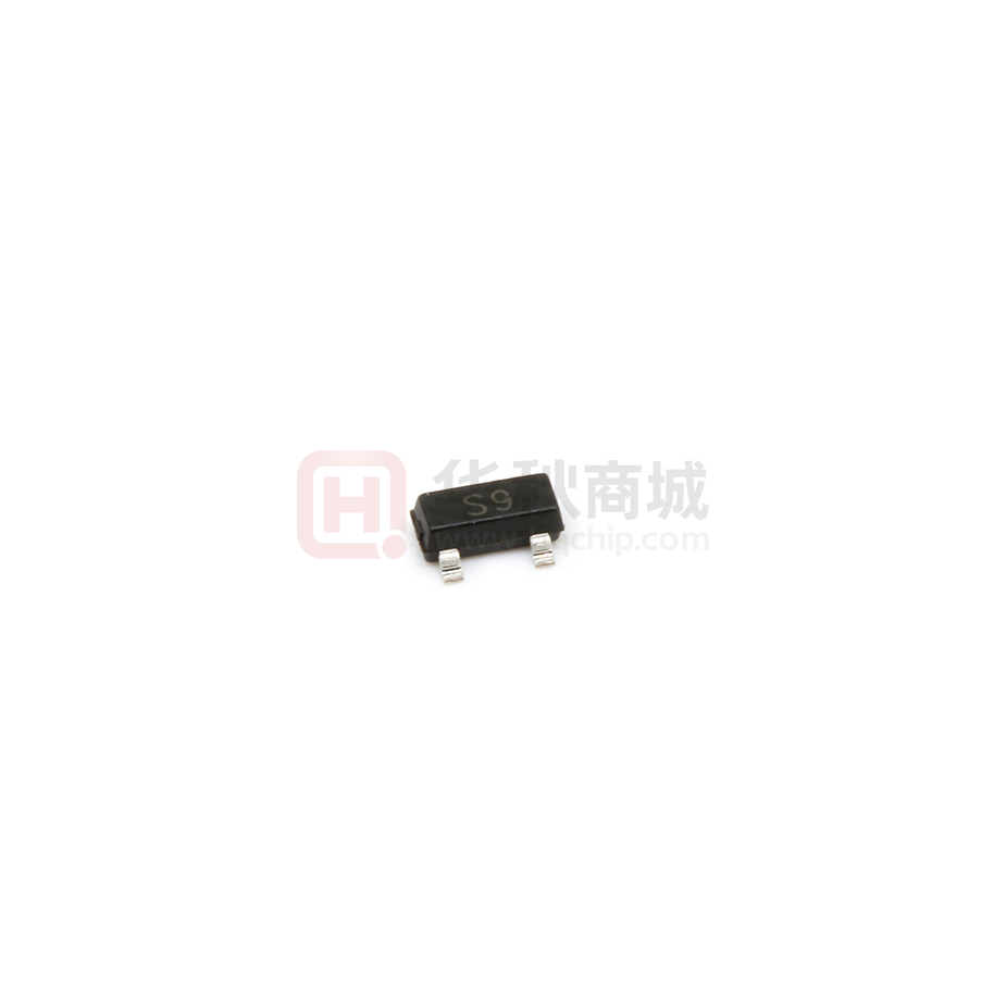
SOT-23
VDS= -60V ID= -2.0A
RDS(ON)= 200mΩ(max) @-10V
Halogen and Antimony Free
1. Gate
Applications
Load Switch and in PWM Applications
Power Management
2.Source
3.Drain
Marking: S9
Schematic Diagram
Drain
3
1
Gate
2 Source
Absolute Maximum Ratings
Ratings at TA =25℃ unless otherwise specified.
Parameter
Value
60
Units
Drain-Source Voltage
Symbol
-VDS
Gate-Source Voltage
VGS
±20
V
Continuous Drain Current
-ID
2
A
Power Dissipation
PD
1.4
W
TJ, TSTG
150, -55 to 150
°C
Symbol
Typ.
Units
RθJA
89
°C/W
Junction and Storage Temperature Range
V
Thermal Characteristics
Parameter
Maximum Junction-to-Ambient
www.pingjingsemi.com
Revision:1.1 Jan-2019
1/7
�PJM2309PSA
P-Channel Power MOSFET
Electrical Characteristics (TC=25℃ unless otherwise specified)
Symbol
Test Condition
Min.
Typ.
Max.
Units
Drain-source breakdown voltage
-V(BR)DSS
VGS = 0V, ID=-250µA
60
--
--
V
Drain to Source Leakage Current
-IDSS
VDS =-60V,VGS = 0V
--
--
1
µA
Gate-body leakage current
IGSS
VGS =±20V, VDS = 0V
--
--
±100
nA
Gate threshold voltage Note1
-VGS(th)
1.5
--
3
V
Drain-source on-resistance Note1
RDS(on)
VGS =-10V, ID =-2A
--
--
200
mΩ
VGS =-4.5V, ID =-1A
--
--
400
mΩ
Forward transconductance Note1
gFS
VDS =-5V, ID =-2A
--
6
--
S
--
850
--
--
65
--
Parameter
Static Characteristics
VDS =VGS, ID =-250µA
Dynamic characteristics
Input Capacitance
Ciss
Output Capacitance
Coss
Reverse Transfer Capacitance
Crss
--
28
--
td(on)
--
7
--
--
3
--
--
28
--
VDS = -30V,VGS = 0V,f=1MHz
pF
Switching Characteristics
Turn-on delay time
Turn-on rise time
Turn-off delay time
tr
td(off)
ID=-1A, VDD=-30V,
VGS=-10V,RGEN =3Ω,
RL =7.5Ω,
ns
Turn-off fall time
tf
--
5.5
--
Total gate charge
Qg
--
22
--
Gate-source charge
Qgs
--
2.5
--
Gate-drain charge
Qgd
--
6
--
-IS
--
--
1.4
A
--
--
1.2
V
VDD =-30V,VGS =-10V,ID =-2A
nC
Source-Drain Diode characteristics
Continuous Source-Drain Diode
Current
Diode Forward voltage
-VDS
VGS =0V, IS=-2A
Notes: 1. Pulse test ; pulse width ≤300μs, duty cycle ≤2%.
www.pingjingsemi.com
Revision:1.1 Jan-2019
2/7
�PJM2309PSA
P-Channel Power MOSFET
Typical Characteristic Curves
2.0
8
1.5
6
I D - Drain Current (A)
I D - Drain Current (A)
VGS = 10 thru 5 V
VGS = 4 V
4
1.0
TC = 25 °C
0.5
2
VGS = 3 V
TC = 125 °C
TC = - 55 °C
0.0
0
0
1
2
3
4
0
5
1
VDS - Drain-to-Source Voltage (V)
2
3
4
5
VGS - Gate-to-Source Voltage (V)
Output Characteristics
Transfer Characteristics
0.8
8
0.6
6
VGS = 4.5 V
Power (W)
R DS(on) - On-Resistance (Ω)
TA = 25 °C
0.4
VGS = 10 V
0.2
4
2
0.0
0
2
4
6
0
0.01
8
0.1
1
100
1000
Time (s)
ID - Drain Current (A)
Single Pulse Power, Junction-to-Ambient
On-Resistance vs. Drain Current and Gate Voltage
10
2.0
ID = 1.25 A
ID = 1.25 A
VDS = 30 V
1.7
VDS = 15 V
6
4
VDS = 45 V
2
VGS = 10 V
(Normalized)
8
R DS(on) - On-Resistance
VGS - Gate-to-Source Voltage (V)
10
1.4
VGS = 4.5 V
1.1
0.8
0
0
5
10
15
Qg - Total Gate Charge (nC)
Gate Charge
www.pingjingsemi.com
Revision:1.1 Jan-2019
20
25
0.5
- 50
- 25
0
25
50
75
100
125
150
TJ - Junction Temperature (°C)
On-Resistance vs. Junction Temperature
3/7
�PJM2309PSA
P-Channel Power MOSFET
100
2.0
ID = 1.25 A
R DS(on) - On-Resistance (Ω)
I S - Source Current (A)
10
TJ = 150 °C
TJ = 25 °C
1
0.1
TJ = - 50 °C
1.6
1.2
0.8
TJ = 125 °C
0.01
0.4
0.001
0.0
0.0
0.3
0.6
0.9
1.2
1.5
TJ = 25 °C
0
2
4
6
8
10
VSD - Source-to-Drain Voltage (V)
VGS - Gate-to-Source Voltage (V)
Source-Drain Diode Forward Voltage
On-Resistance vs. Gate-to-Source Voltage
10
0.6
10 µs
Limited by RDS(on)*
ID = 250 µA
ID = 1 mA
0.2
0.0
I D - Drain Current (A)
VGS(th) Variance (V)
0.4
1
100 µs
1 ms
10 ms
0.1
- 0.2
100 ms
TA = 25 °C
Single Pulse
- 0.4
- 50
- 25
0
25
50
75
100
125
150
0.01
0.1
1 s, 10 s
100 s, DC
1
100
10
VDS - Drain-to-Source Voltage (V)
* VGS > minimum VGS at which RDS(on) is specified
TJ - Temperature (°C)
Threshold Voltage
Safe Operating Area, Junction-to-Ambient
1
Normalized Effective Transient
Thermal Impedance
Duty Cycle = 0.5
0.2
0.1
0.1
Notes:
0.05
PDM
0.02
t1
t2
1. Duty Cycle, D =
t1
t2
2. Per Unit Base = RthJA = 166 °C/W
3. TJM - TA = PDMZthJA(t)
Single Pulse
0.01
10 -4
4. Surface Mounted
10 -3
10 -2
10 -1
1
Square Wave Pulse Duration (s)
10
100
1000
Normalized Thermal Transient Impedance, Junction-to-Ambient
www.pingjingsemi.com
Revision:1.1 Jan-2019
4/7
�PJM2309PSA
P-Channel Power MOSFET
Package Outline
SOT-23
0.8
Max.
1.025
1.150
A1
0.000
0.050
0.100
b
c
D
0.300
0.080
2.800
0.400
0.115
2.900
0.500
0.150
3.000
E
1.200
1.300
1.400
HE
2.250
2.400
2.550
e
1.800
1.900
2.000
0.550REF
L1
L
0.300
0o
θ
0.500
8o
2.2
Typ.
0.900
0.8
1.0
Min.
A
1.0
Dimensions in millimeter
Symbol
1.9
SOT-23 (TO-236)
Recommended soldering pad
Ordering Information
Device
Package
Shipping
PJM2309PSA
SOT-23
3000PCS/Reel&Tape
www.pingjingsemi.com
Revision:1.1 Jan-2019
5/7
�PJM2309PSA
P-Channel Power MOSFET
Conditions of Soldering And Storage
Recommended condition of reflow soldering
Recommended peak temperature is over 245 ℃. If peak temperature is below 245 ℃, you may adjust
the following parameters:
Time length of peak temperature (longer)
Time length of soldering (longer)
Thickness of solder paste (thicker)
Conditions of hand soldering
Temperature: 370 ℃
Time: 3s max.
Times: one time
Storage conditions
Temperature
5 to 40 ℃
Humidity
30 to 80% RH
Recommended period
One year after manufacturing
www.pingjingsemi.com
Revision:1.1 Jan-2019
6/7
�PJM2309PSA
P-Channel Power MOSFET
Package Specifications
The method of packaging
Cover Tape
SOT-23 (TO-236)
3,000 pcs per reel
1
3
2
Carrier Tape
30,000 pcs per box
10 reels per box
220
195
0
435
21
43
5
120,000 pcs per carton
4 boxes per carton
210
Embossed tape and reel data
D
A
T2
T1
4.0
4.0
B
8.0
C
E
1Pin
G
N
Tape (8mm)
F
Reel (7'')
www.pingjingsemi.com
Revision:1.1 Jan-2019
Symbol
A
B
C
E
F
D
T1
T2
N
G
Value (unit: mm)
Ø 177.8±1
2.7±0.2
Ø 13.5±0.2
Ø 54.5±0.2
12.3±0.3
9.6+2/-0.3
1.0±0.2
1.2±0.2
3.15±0.1
1.25±0.1
7/7
�
很抱歉,暂时无法提供与“PJM2309PSA”相匹配的价格&库存,您可以联系我们找货
免费人工找货- 国内价格
- 10+0.39669
- 100+0.30964
- 300+0.26601
- 3000+0.23339
- 6000+0.20726
- 9000+0.19419
- 国内价格
- 5+0.24990
- 20+0.22785
- 100+0.20580
- 500+0.18375
- 1000+0.17346
- 2000+0.16611