Important notice
Dear Customer,
On 7 February 2017 the former NXP Standard Product business became a new company with the
tradename Nexperia. Nexperia is an industry leading supplier of Discrete, Logic and PowerMOS
semiconductors with its focus on the automotive, industrial, computing, consumer and wearable
application markets
In data sheets and application notes which still contain NXP or Philips Semiconductors references, use
the references to Nexperia, as shown below.
Instead of http://www.nxp.com, http://www.philips.com/ or http://www.semiconductors.philips.com/,
use http://www.nexperia.com
Instead of sales.addresses@www.nxp.com or sales.addresses@www.semiconductors.philips.com, use
salesaddresses@nexperia.com (email)
Replace the copyright notice at the bottom of each page or elsewhere in the document, depending on
the version, as shown below:
- © NXP N.V. (year). All rights reserved or © Koninklijke Philips Electronics N.V. (year). All rights
reserved
Should be replaced with:
- © Nexperia B.V. (year). All rights reserved.
If you have any questions related to the data sheet, please contact our nearest sales office via e-mail
or telephone (details via salesaddresses@nexperia.com). Thank you for your cooperation and
understanding,
Kind regards,
Team Nexperia
�PESD5V0S1UJ; PESD12VS1UJ
Unidirectional ESD protection for transient voltage
suppression
Rev. 01 — 3 June 2009
Product data sheet
1. Product profile
1.1 General description
Unidirectional ElectroStatic Discharge (ESD) protection diodes in a very small
Surface-Mounted Device (SMD) plastic package designed to protect one signal line
from the damage caused by ESD and transient overvoltage.
Table 1.
Product overview
Type number
PESD5V0S1UJ
Package
Configuration
NXP
JEITA
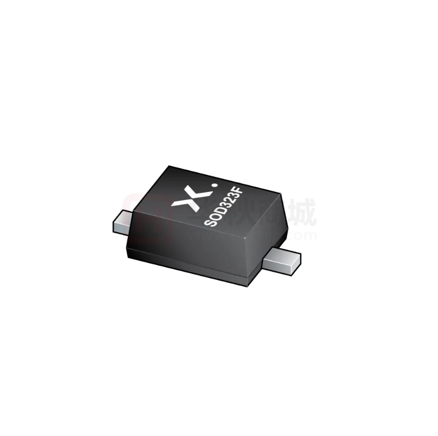
SOD323F
SC-90
single
PESD12VS1UJ
1.2 Features
n Transient Voltage Suppression (TVS)
protection of one line
n Max. peak pulse power: PPP = 890 W
n Low clamping voltage: VCL = 19 V
n Low leakage current: IRM = 300 nA
n ESD protection up to 30 kV
n IEC 61000-4-2; level 4 (ESD)
n IEC 61000-4-5 (surge); IPP = 47 A
n AEC-Q101 qualified
1.3 Applications
n Computers and peripherals
n Audio and video equipment
n Cellular handsets and accessories
n Communication systems
n Portable electronics
n Medical and industrial equipment
1.4 Quick reference data
Table 2.
Quick reference data
Tamb = 25 °C unless otherwise specified.
Symbol
Parameter
VRWM
reverse standoff voltage
Cd
Conditions
Min
Typ
Max
Unit
PESD5V0S1UJ
-
-
5
V
PESD12VS1UJ
-
-
12
V
PESD5V0S1UJ
-
480
530
pF
PESD12VS1UJ
-
160
180
pF
diode capacitance
f = 1 MHz; VR = 0 V
�PESD5V0S1UJ; PESD12VS1UJ
NXP Semiconductors
Unidirectional ESD protection for transient voltage suppression
2. Pinning information
Table 3.
Pinning
Pin
Description
1
cathode
2
anode
Simplified outline
Graphic symbol
[1]
1
2
1
2
006aaa152
[1]
The marking bar indicates the cathode.
3. Ordering information
Table 4.
Ordering information
Type number
PESD5V0S1UJ
Package
Name
Description
Version
SC-90
plastic surface-mounted package; 2 leads
SOD323F
PESD12VS1UJ
4. Marking
Table 5.
Marking codes
Type number
Marking code
PESD5V0S1UJ
1Q
PESD12VS1UJ
1R
5. Limiting values
Table 6.
Limiting values
In accordance with the Absolute Maximum Rating System (IEC 60134).
Symbol
PPP
IPP
Parameter
Conditions
peak pulse power
tp = 8/20 µs
Max
Unit
PESD5V0S1UJ
-
890
W
PESD12VS1UJ
-
600
W
PESD5V0S1UJ
-
47
A
PESD12VS1UJ
-
22.5
A
peak pulse current
tp = 8/20 µs
PESD5V0S1UJ_PESD12VS1UJ_1
Product data sheet
Min
[1][2]
[1][2]
© NXP B.V. 2009. All rights reserved.
Rev. 01 — 3 June 2009
2 of 14
�PESD5V0S1UJ; PESD12VS1UJ
NXP Semiconductors
Unidirectional ESD protection for transient voltage suppression
Table 6.
Limiting values …continued
In accordance with the Absolute Maximum Rating System (IEC 60134).
Symbol
Ptot
Parameter
Conditions
total power dissipation
Tamb ≤ 25 °C
Min
Max
Unit
[3]
-
420
mW
[4]
-
720
mW
Tj
junction temperature
-
150
°C
Tamb
ambient temperature
−55
+150
°C
Tstg
storage temperature
−65
+150
°C
[1]
Non-repetitive current pulse 8/20 µs exponential decay waveform according to IEC 61000-4-5.
[2]
Soldering point of cathode tab.
[3]
Device mounted on an FR4 Printed-Circuit Board (PCB), single-sided copper, tin-plated and standard
footprint.
[4]
Device mounted on an FR4 PCB, single-sided copper, tin-plated, mounting pad for cathode 1 cm2.
Table 7.
ESD maximum ratings
Tamb = 25 °C unless otherwise specified.
Symbol
VESD
[1]
Parameter
Conditions
electrostatic discharge voltage
Min
Max
Unit
-
30
kV
machine model
-
400
V
MIL-STD-883 (human
body model)
-
16
kV
IEC 61000-4-2
(contact discharge)
Device stressed with ten non-repetitive ESD pulses.
Table 8.
ESD standards compliance
Standard
Conditions
IEC 61000-4-2; level 4 (ESD)
> 15 kV (air); > 8 kV (contact)
MIL-STD-883; class 3 (human body model)
> 4 kV
PESD5V0S1UJ_PESD12VS1UJ_1
Product data sheet
[1]
© NXP B.V. 2009. All rights reserved.
Rev. 01 — 3 June 2009
3 of 14
�PESD5V0S1UJ; PESD12VS1UJ
NXP Semiconductors
Unidirectional ESD protection for transient voltage suppression
001aaa631
IPP
001aaa630
120
100 %
90 %
100 % IPP; 8 µs
IPP
(%)
80
e−t
50 % IPP; 20 µs
40
10 %
0
10
20
30
30 ns
40
t (µs)
Fig 1.
t
tr = 0.7 ns to 1 ns
0
60 ns
8/20 µs pulse waveform according to
IEC 61000-4-5
Fig 2.
ESD pulse waveform according to
IEC 61000-4-2
6. Thermal characteristics
Table 9.
Symbol
Rth(j-a)
Rth(j-sp)
Thermal characteristics
Parameter
Conditions
thermal resistance from
junction to ambient
in free air
thermal resistance from
junction to solder point
Typ
Max
Unit
-
-
290
K/W
[2]
-
-
170
K/W
[3]
-
-
35
K/W
[1]
Device mounted on an FR4 PCB, single-sided copper, tin-plated and standard footprint.
[2]
Device mounted on an FR4 PCB, single-sided copper, tin-plated, mounting pad for cathode 1 cm2.
[3]
Soldering point of cathode tab.
PESD5V0S1UJ_PESD12VS1UJ_1
Product data sheet
Min
[1]
© NXP B.V. 2009. All rights reserved.
Rev. 01 — 3 June 2009
4 of 14
�PESD5V0S1UJ; PESD12VS1UJ
NXP Semiconductors
Unidirectional ESD protection for transient voltage suppression
7. Characteristics
Table 10. Characteristics
Tamb = 25 °C unless otherwise specified.
Symbol
Parameter
VRWM
reverse standoff voltage
IRM
Conditions
-
-
5
V
-
12
V
VRWM = 5 V
-
0.3
4
µA
VRWM = 12 V
-
很抱歉,暂时无法提供与“PESD5V0S1UJF”相匹配的价格&库存,您可以联系我们找货
免费人工找货