PUSB3F99
ESD protection for ultra high-speed interfaces
Rev. 1 — 15 December 2017
1
Product data sheet
Product profile
1.1 General description
The device is designed to protect high-speed interfaces such as SuperSpeed USB,
High-Definition Multimedia Interface (HDMI), DisplayPort, external Serial Advanced
Technology Attachment (eSATA) and Low Voltage Differential Signaling (LVDS)
interfaces against ElectroStatic Discharge (ESD).
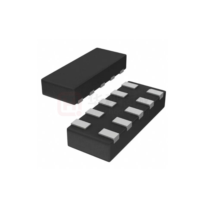
The device includes four high-level ESD protection diode structures for ultra high-speed
signal lines and is encapsulated in a leadless small DFN2510A-10 (SOT1176-1) plastic
package.
All signal lines are protected by a special diode configuration offering ultra low line
capacitance of only 0.5 pF. These diodes utilize a unique snap-back structure in order to
provide protection to downstream components from ESD voltages up to ±10 kV contact
exceeding IEC 61000-4-2, level 4.
1.2 Features and benefits
• System ESD protection for USB 2.0 and SuperSpeed USB 3.1, HDMI 2.0, DisplayPort,
eSATA and LVDS
• All signal lines with integrated rail-to-rail clamping diodes for downstream ESD
protection of ±10 kV exceeding IEC 61000-4-2, level 4
• Matched 0.5 mm trace spacing
• Signal lines with ≤ 0.05 pF matching capacitance between signal pairs
• Line capacitance of only 0.5 pF for each channel
• Design-friendly ‘pass-through’ signal routing
1.3 Applications
The device is designed for high-speed receiver and transmitter port protection:
•
•
•
•
TVs and monitors
DVD recorders and players
Notebooks, main board graphic cards and ports
Set-top boxes and game consoles
�PUSB3F99
Nexperia
ESD protection for ultra high-speed interfaces
2
Pinning information
Table 1. Pinning
Pin
Symbol
Description
1
CH1
channel 1 ESD protection
2
CH2
channel 2 ESD protection
3
GND
ground
4
CH3
channel 3 ESD protection
5
CH4
channel 4 ESD protection
6
n.c.
not connected
7
n.c.
not connected
8
GND
ground
9
n.c.
not connected
10
n.c.
not connected
3
Simplified outline
10
9
8
7
6
Graphic symbol
1
2
4
5
1
2
3
4
5
Transparent top view
3, 8
018aaa001
Ordering information
Table 2. Ordering information
Type number
Package
PUSB3F99
4
Name
Description
Version
DFN2510A-10
plastic extremely thin small outline package; no leads;10
terminals; body 1 × 2.5 × 0.5 mm
SOT1176-1
Marking
Table 3. Marking codes
Type number
Marking code
PUSB3F99
96
5
Limiting values
Table 4. Limiting values
In accordance with the Absolute Maximum Rating System (IEC 60134).
Symbol
Parameter
Conditions
VI
input voltage
VESD
electrostatic discharge voltage
Min
Max
Unit
-0.5
+3.3
V
• contact discharge
-10
+10
kV
• air discharge
-15
+15
kV
IEC 61000-4-2, level 4
[1]
Tamb
ambient temperature
-40
+85
°C
Tstg
storage temperature
-55
+125
°C
[1]
All pins to ground.
PUSB3F99
Product data sheet
All information provided in this document is subject to legal disclaimers.
Rev. 1 — 15 December 2017
© Nexperia B.V. 2017. All rights reserved.
2 / 12
�PUSB3F99
Nexperia
ESD protection for ultra high-speed interfaces
6
Characteristics
Table 5. Characteristics
Tamb = 25 °C unless otherwise specified.
Symbol
Parameter
Conditions
Min
Typ
Max
Unit
VBR
breakdown voltage
II = 1 mA
6
-
-
V
ILR
reverse leakage current
per channel; VI = 3 V
-
-
1
μA
VF
forward voltage
II = 1 mA
-
0.7
-
V
Cline
line capacitance
[1]
-
0.5
0.6
pF
ΔCline
line capacitance difference
[1]
-
0.05
-
pF
rdyn
dynamic resistance
-
0.41
-
Ω
-
0.26
-
Ω
-
0.43
-
Ω
-
0.28
-
Ω
-
4.6
-
V
-
-2.2
-
V
f = 1 MHz; VI = 3.3 V
f = 1 MHz; VI = 3.3 V
surge
[2]
• positive transient
• negative transient
TLP
[3]
• positive transient
• negative transient
VCL
clamping voltage
IPP = 5.2 A
[2]
• positive transient
IPP = -4.4 A
• negative transient
[1]
[2]
[3]
[2]
This parameter is guaranteed by design.
According to IEC 61000-4-5 (8/20 μs current waveform).
100 ns Transmission Line Pulse (TLP); 50 Ω; pulser at 80 ns.
PUSB3F99
Product data sheet
All information provided in this document is subject to legal disclaimers.
Rev. 1 — 15 December 2017
© Nexperia B.V. 2017. All rights reserved.
3 / 12
�PUSB3F99
Nexperia
ESD protection for ultra high-speed interfaces
6.1
aaa-009367
2
Sdd21
(dB)
aaa-009368
1.2
a
-2
0.8
-6
0.4
-10
-14
106
107
108
109
f (MHz)
0
1010
0
1
2
3
4
VI (V)
5
differential mode
Figure 1. Insertion loss; typical values
Figure 2. Relative capacitance as a function of input
voltage; typical values
aaa-009369
0
aaa-009370
120
Zdif
(Ω)
Sdd21
(dB)
110
-20
(2)
100
-40
90
(1)
-60
106
107
108
109
f (MHz)
1010
Sdd21 normalized to 100 Ω;differential pairs CH1/CH2
versus CH3/CH4
Figure 3. Crosstalk; typical values
80
40.0
40.5
41.0
41.5
t (ns)
42.0
tr = 200 ps; differential pair CH1 + CH2
(1) PUSB3F99 on reference board
(2) Reference board without device under test (DUT)
Figure 4. Differential Time Domain Reflectometer (TDR)
plot; typical values
PUSB3F99
Product data sheet
All information provided in this document is subject to legal disclaimers.
Rev. 1 — 15 December 2017
© Nexperia B.V. 2017. All rights reserved.
4 / 12
�PUSB3F99
Nexperia
ESD protection for ultra high-speed interfaces
Data rate: 10 Gbit/s; Vertical scale: 200 mV/div; Horizontal scale: 20 ps/div
3.1 dB de-emphasis
2.2 dB pre-shoot
Figure 5. USB 3.1 eye diagram, Printed-Circuit Board (PCB) with PUSB3F99
Data rate: 10 Gbit/s; Vertical scale: 200 mV/div; Horizontal scale: 20 ps/div
3.1 dB de-emphasis
2.2 dB pre-shoot
Figure 6. USB 3.1 eye diagram, PCB without PUSB3F99 (reference)
PUSB3F99
Product data sheet
All information provided in this document is subject to legal disclaimers.
Rev. 1 — 15 December 2017
© Nexperia B.V. 2017. All rights reserved.
5 / 12
�PUSB3F99
Nexperia
ESD protection for ultra high-speed interfaces
aaa-014159
Test frequency: 148.5 MHz
Differential swing voltage: 810 mV
Horizontal scale: 34 ps/div
Figure 7. HDMI 2.0 TP1 eye diagram, PCB with PUSB3F99 (2160p, 60 Hz
aaa-014160
Test frequency: 148.5 MHz
Differential swing voltage: 800 mV
Horizontal scale: 34 ps/div
Figure 8. HDMI 2.0 TP1 eye diagram, PCB without PUSB3F99 (2160p, 60 Hz, reference)
PUSB3F99
Product data sheet
All information provided in this document is subject to legal disclaimers.
Rev. 1 — 15 December 2017
© Nexperia B.V. 2017. All rights reserved.
6 / 12
�PUSB3F99
Nexperia
ESD protection for ultra high-speed interfaces
aaa-014161
Test frequency: 148.5 MHz
Differential swing voltage: 809 mV
Horizontal scale: 34 ps/div
Remark: Measured at Test Point 2 (TP2) worst cable emulator, reference cable equalizer and worst case positive skew.
Figure 9. HDMI 2.0 TP2 eye diagram, PCB with PUSB3F99 (2160p, 60 Hz)
aaa-014162
Test frequency: 148.5 MHz
Differential swing voltage: 820 mV
Horizontal scale: 34 ps/div
Remark: Measured at Test Point 2 (TP2) worst cable emulator, reference cable equalizer and worst case positive skew.
Figure 10. HDMI 2.0 TP2 eye diagram, PCB without PUSB3F99 (2160p, 60 Hz, reference)
PUSB3F99
Product data sheet
All information provided in this document is subject to legal disclaimers.
Rev. 1 — 15 December 2017
© Nexperia B.V. 2017. All rights reserved.
7 / 12
�PUSB3F99
Nexperia
ESD protection for ultra high-speed interfaces
aaa-009371
6
IPP
(A)
aaa-009372
0
IPP
(A)
4
-2
2
-4
0
0
2
4
VCL (V)
-6
-2.5
6
-2.0
-1.5
-1.0
-0.5
0
VCL (V)
IEC 61000-4-5; tp = 8/20 μs; positive pulse
IEC 61000-4-5; tp = 8/20 μs; negative pulse
Figure 11. Dynamic resistance with positive clamping;
typical values
Figure 12. Dynamic resistance with negative clamping;
typical values
aaa-009373
14
I
(A)
12
I
(A)
-2
10
-4
8
-6
6
-8
4
-10
2
-12
0
0
4
8
VCL (V)
12
aaa-009374
0
-14
-6
-4
-2
VCL (V)
0
tp = 100 ns; Transmission Line Pulse (TLP)
tp = 100 ns; Transmission Line Pulse (TLP)
Figure 13. Dynamic resistance with positive clamping;
typical values
Figure 14. Dynamic resistance with negative clamping;
typical values
The device uses an advanced clamping structure showing a negative dynamic
resistance. This snap-back behavior strongly reduces the clamping voltage to the system
behind the ESD protection during an ESD event. Do not connect unlimited DC current
sources to the data lines to avoid keeping the ESD protection device in snap-back state
after exceeding breakdown voltage (due to an ESD pulse for instance).
PUSB3F99
Product data sheet
All information provided in this document is subject to legal disclaimers.
Rev. 1 — 15 December 2017
© Nexperia B.V. 2017. All rights reserved.
8 / 12
�PUSB3F99
Nexperia
ESD protection for ultra high-speed interfaces
7
Application information
The device is designed to provide high-level ESD protection for high-speed serial data
buses such as HDMI, DisplayPort, eSATA and LVDS data lines.
When designing the Printed-Circuit Board (PCB), give careful consideration to
impedance matching and signal coupling. Do not connect the signal lines to unlimited
current sources like, for example, a battery.
8
Package outline
Table 6. Package outline
1.1
0.9
5
0.2 min
0.127
6
2.6
2
2.4
0.25
0.15
0.5
1
10
0.45
0.35
Dimensions in mm
0.4
0.3
0.05 max
0.5 max
12-05-23
Figure 15. Package outline DFN2510A-10 (SOT1176-1)
PUSB3F99
Product data sheet
All information provided in this document is subject to legal disclaimers.
Rev. 1 — 15 December 2017
© Nexperia B.V. 2017. All rights reserved.
9 / 12
�PUSB3F99
Nexperia
ESD protection for ultra high-speed interfaces
9
Soldering
Table 7. Soldering
Footprint information for reflow soldering of DFN2510A-10 package
SOT1176-1
Hx
C
Hy
Ay
By
0.05
D
P
0.05
Generic footprint pattern
Refer to the package outline drawing for actual layout
solder land
solder paste deposit
solder land plus solder paste
occupied area
solder resist
Dimensions in mm
P
Ay
By
C
D
Hx
Hy
0.5
1.25
0.3
0.475
0.2
2.45
1.5
Remark:
Stencil of 75 m is recommended.
A stencil of 75 m gives an aspect ratio of 0.77
With a stencil of 100 m one will obtain an aspect ratio of 0.58
sot1176-1_fr
Figure 16. Reflow soldering footprint DFN2510A-10 (SOT1176-1)
PUSB3F99
Product data sheet
All information provided in this document is subject to legal disclaimers.
Rev. 1 — 15 December 2017
© Nexperia B.V. 2017. All rights reserved.
10 / 12
�PUSB3F99
Nexperia
ESD protection for ultra high-speed interfaces
10 Revision history
Table 8. Revision history
Document ID
Release date
Data sheet status
Change notice
Supersedes
PUSB3F99 v.1
20171215
Product data sheet
-
-
PUSB3F99
Product data sheet
All information provided in this document is subject to legal disclaimers.
Rev. 1 — 15 December 2017
© Nexperia B.V. 2017. All rights reserved.
11 / 12
�PUSB3F99
Nexperia
ESD protection for ultra high-speed interfaces
Contents
1
1.1
1.2
1.3
2
3
4
5
6
6.1
7
8
9
10
Product profile .................................................... 1
General description ............................................1
Features and benefits ........................................1
Applications ........................................................1
Pinning information ............................................ 2
Ordering information .......................................... 2
Marking .................................................................2
Limiting values .................................................... 2
Characteristics .................................................... 3
............................................................................ 4
Application information ......................................9
Package outline ...................................................9
Soldering ............................................................10
Revision history ................................................ 11
Please be aware that important notices concerning this document and the product(s)
described herein, have been included in section 'Legal information'.
© Nexperia B.V. 2017.
All rights reserved.
For more information, please visit: http://www.nexperia.com
For sales office addresses, please send an email to: salesaddresses@nexperia.com
Date of release: 15 December 2017
Document identifier: PUSB3F99
�
很抱歉,暂时无法提供与“PUSB3F99X”相匹配的价格&库存,您可以联系我们找货
免费人工找货- 国内价格
- 1+3.80160
- 10+3.74760
- 30+3.71520
- 100+3.69360