74ABT32
Quad 2-input OR gate
Rev. 3 — 12 August 2016
Product data sheet
1. General description
The 74ABT32 high-performance BiCMOS device combines low static and dynamic power
dissipation with high speed and high output drive.
The 74ABT32 is a quad 2-input OR gate.
2. Features and benefits
Latch-up protection exceeds 500 mA per JESD78B class II level A
ESD protection:
HBM JESD22-A114F exceeds 2000 V
MM JESD22-A115-A exceeds 200 V
Multiple package options
Specified from 40 C to +85 C
3. Ordering information
Table 1.
Ordering information
Type number
Package
Temperature range Name
Description
Version
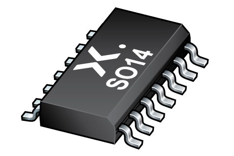
74ABT32D
40 C to +85 C
SO14
plastic small outline package; 14 leads; body width
3.9 mm
SOT108-1
74ABT32DB
40 C to +85 C
SSOP14
plastic shrink small outline package; 14 leads; body
width 5.3 mm
SOT337-1
74ABT32PW
40 C to +85 C
TSSOP14
plastic thin shrink small outline package; 14 leads;
body width 4.4 mm
SOT402-1
�74ABT32
Nexperia
Quad 2-input OR gate
4. Functional diagram
�
�
�
�
�
�
�
�
�
�
�$
�
�%
�
�$
�
�%
�
�$
��
�%
��
�$
��
�%
�<
�
�<
�
�
�
��
�<
�
�<
��
$
��
��
<
��
%
PQD���
PQD���
Fig 1.
�
Logic symbol
Fig 2.
IEC logic symbol
PQD���
Fig 3.
Logic diagram (one gate)
5. Pinning information
5.1 Pinning
��$%7��
��$%7��
�$
�
�� 9&&
�%
�
�� �%
�$
�
�<
�
�� �$
�%
�
�� 9&&
�� �%
�$
�
�� �<
�<
�
�� �$
�$
�
�� �<
�� �%
�%
�
�� �%
�
�<
�
�
�$
*1'
�
�
�<
�%
�<
*1'
�
�
�
�
�$
�<
DDD�������
DDD�������
Fig 4.
Pin configuration for SO14
Fig 5.
Pin configuration for SSOP14 and TSSOP14
5.2 Pin description
Table 2.
Pin description
Symbol
Pin
Description
1A to 4A
1, 4, 9, 12
data input
1B to 4B
2, 5, 10, 13
data input
1Y to 4Y
3, 6, 8, 11
data output
GND
7
ground (0 V)
VCC
14
supply voltage
74ABT32
Product data sheet
All information provided in this document is subject to legal disclaimers.
Rev. 3 — 12 August 2016
©
Nexperia B.V. 2017. All rights reserved
2 of 12
�74ABT32
Nexperia
Quad 2-input OR gate
6. Functional description
Table 3.
Function selection[1]
Input
Output
nA
nB
nY
L
L
L
X
H
H
H
X
H
H
H
H
[1]
H = HIGH voltage level; L = LOW voltage level; X = don’t care
7. Limiting values
Table 4.
Limiting values
In accordance with the Absolute Maximum Rating System (IEC 60134).
Symbol
Parameter
Conditions
VCC
supply voltage
VI
input voltage
VO
output voltage
output in Off or High state
IIK
input clamping current
IOK
IO
Min
Max
Unit
0.5
+7.0
V
[1]
1.2
+7.0
V
[1]
0.5
+5.5
V
VI < 0 V
18
-
mA
output clamping current
VO < 0 V
50
-
mA
output current
output in LOW-state
-
40
mA
-
150
C
65
+150
C
Tj
junction temperature
Tstg
storage temperature
[2]
[1]
The input and output voltage ratings may be exceeded if the input and output current ratings are observed.
[2]
The performance capability of a high-performance integrated circuit in conjunction with its thermal environment can create junction
temperatures which are detrimental to reliability. The maximum junction temperature of this integrated circuit should not exceed 150 C.
8. Recommended operating conditions
Table 5.
Operating conditions
Voltages are referenced to GND (ground = 0 V).
Symbol
Parameter
VCC
supply voltage
VI
input voltage
VIH
HIGH-level input voltage
Conditions
Min
Typ
Max
Unit
4.5
-
5.5
V
0
-
VCC
V
2.0
-
-
V
V
VIL
LOW-level input voltage
-
-
0.8
IOH
HIGH-level output current
15
-
-
mA
IOL
LOW-level output current
-
-
20
mA
t/V
input transition rise and fall rate
0
-
10
ns/V
Tamb
ambient temperature
40
-
+85
C
74ABT32
Product data sheet
in free air
All information provided in this document is subject to legal disclaimers.
Rev. 3 — 12 August 2016
©
Nexperia B.V. 2017. All rights reserved
3 of 12
�74ABT32
Nexperia
Quad 2-input OR gate
9. Static characteristics
Table 6.
Static characteristics
Symbol
Parameter
25 C
Conditions
40 C to +85 C Unit
Min
Typ
Max
Min
Max
1.2
0.9
-
1.2
-
V
2.5
2.9
-
2.5
-
V
0.5
-
0.5
V
VIK
input clamping voltage VCC = 4.5 V; IIK = 18 mA
VOH
HIGH-level output
voltage
VCC = 4.5 V; IOH = 15 mA;
VI = VIL or VIH
VOL
LOW-level output
voltage
VCC = 4.5 V; IOL = 20 mA;
VI = VIL or VIH
-
0.35
II
input leakage current
VCC = 5.5 V; VI = GND or 5.5 V
-
0.01 1.0
-
1.0
A
IOFF
power-off leakage
current
VCC = 0 V; VI or VO 4.5 V
-
5.0
100
-
100
A
ICEX
output high leakage
current
HIGH-state; VO = 5.5 V;
VCC = 5.5 V; VI = GND or VCC
-
5.0
50
-
50
A
IO
output current
VCC = 5.5 V; VO = 2.5 V
50
75
180
50
180
mA
ICC
supply current
VCC = 5.5 V; VI = GND or VCC
-
2
50
-
50
A
-
0.25
500
-
500
A
-
3
-
-
-
pF
40 C to +85 C;
VCC = 5.0 V 0.5 V
Unit
ICC
additional supply
current
per input pin; VCC = 5.5 V;
one input at 3.4 V;
other inputs at VCC or GND
CI
input capacitance
VI = 0 V or VCC
[1]
[2]
[1]
Not more than one output should be tested at a time, and the duration of the test should not exceed one second.
[2]
This is the increase in supply current for each input at 3.4 V.
10. Dynamic characteristics
Table 7.
Dynamic characteristics
GND = 0 V; for test circuit, see Figure 7.
Symbol Parameter
25 C; VCC = 5.0 V
Conditions
Min
Typ
Max
Min
Max
tPLH
LOW to HIGH
propagation delay
nA, nB to nY; see Figure 6
1.0
2.3
3.4
1.0
3.8
ns
tPHL
HIGH to LOW
propagation delay
nA, nB to nY; see Figure 6
1.0
1.9
2.9
1.0
3.2
ns
tsk(o)
output skew time
-
0.4
0.5
-
0.5
ns
[1]
[1]
Skew between any two outputs of the same package switching in the same direction. This parameter is guaranteed by design.
74ABT32
Product data sheet
All information provided in this document is subject to legal disclaimers.
Rev. 3 — 12 August 2016
©
Nexperia B.V. 2017. All rights reserved
4 of 12
�74ABT32
Nexperia
Quad 2-input OR gate
11. Waveforms
9,
90
Q$��Q%�LQSXW
*1'
W 3+/�
W 3/+
90
Q
很抱歉,暂时无法提供与“74ABT32D,118”相匹配的价格&库存,您可以联系我们找货
免费人工找货- 国内价格 香港价格
- 1+8.226591+1.06189
- 10+5.9094510+0.76280
- 25+5.3257825+0.68746
- 100+4.68434100+0.60466
- 250+4.37916250+0.56527
- 500+4.19496500+0.54149
- 1000+4.187891000+0.54058
- 国内价格 香港价格
- 2500+3.656592500+0.47200
- 5000+3.564865000+0.46016
- 7500+3.518937500+0.45423
- 12500+3.4680412500+0.44766
- 17500+3.4383017500+0.44382
- 25000+3.4096825000+0.44013