物料型号:74AXP1G98
器件简介:
- 74AXP1G98是一款带有施密特触发器输入的可配置多功能门器件。
- 设备可以配置为以下逻辑功能:多路选择器(MUX)、与门(AND)、或门(OR)、与非门(NAND)、或非门(NOR)、反相器和缓冲器。
- 所有输入可以直接连接到VCC或GND。
- 该设备在整个VCC范围(0.7 V至2.75 V)内确保了非常低的静态和动态功耗。
- 使用IOFF电路在部分电源关闭应用中禁用输出,防止在关闭电源时通过设备产生潜在的有害回流电流。
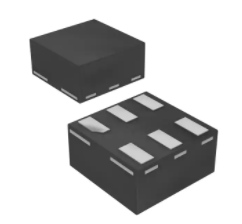
引脚分配:
- 引脚1:数据输入B
- 引脚2:地(GND,0V)
- 引脚3:数据输入A
- 引脚4:数据输出Y
- 引脚5:供电电压Vcc
- 引脚6:数据输入C
参数特性:
- 供电电压范围宽:0.7 V至2.75 V
- 输入电容低:典型值0.5 pF
- 输出电容低:典型值1.0 pF
- 动态功耗低:在VCC = 1.2 V时,CPD = 2.7 pF(典型值)
- 静态功耗低:在最高85°C时,ICC = 1.0 μA(最大值)
- 高抗噪声能力
- 符合JEDEC标准的ESD保护等级
功能详解:
- 提供了逻辑功能选择表,可以配置为2输入MUX、2输入NAND、2输入NOR等不同的逻辑门。
- 提供了逻辑符号和功能表,展示了不同输入条件下的输出Y的状态。
应用信息:
- 设备接受高达2.75V的输入电压。
- 在部分电源关闭模式下,IOFF电路提供了操作。
- 提供了多种封装选项,并规定了从-40°C到+85°C的温度范围。
封装信息:
- 提供了74AXP1G98GM、74AXP1G98GN和74AXP1G98GS三种型号的封装信息,分别对应不同的温度范围和封装类型。


 工商网监
湘ICP备2023018690号
工商网监
湘ICP备2023018690号