物料型号:74LVC1G58
器件简介:
74LVC1G58是一种低功耗、可配置的多功能门电路。它可以根据3位输入的八种模式来确定输出状态。用户可以选择逻辑功能,包括与门(AND)、或门(OR)、与非门(NAND)、或非门(NOR)、异或门(XOR)、反相器(inverter)和缓冲器(buffer)。所有输入可以连接到VCC或GND。该设备能够在3.3V或5V设备中驱动输入,允许在3.3V和5V混合环境中使用。此外,该设备还具备部分断电应用的全面规范,使用IOFF电路在断电时禁用输出,防止通过设备产生有害的反向电流。所有输入(A, B和C)都是施密特触发器输入,能够将缓慢变化的输入信号转换为清晰、无抖动的输出信号。
引脚分配:
- B(1号引脚):数据输入
- GND(2号引脚):地(0V)
- A(3号引脚):数据输入
- Y(4号引脚):数据输出
- Vcc(5号引脚):供电电压
- (6号引脚):数据输入
参数特性:
- 宽供电电压范围:1.65V至5.5V
- 5V容限输入/输出,用于与5V逻辑接口
- 高抗噪声能力
- 符合JEDEC标准
- ESD保护:人体模型(HBM)超过2000V,机器模型(MM)超过200V
- 输出驱动能力:±24mA(VCC = 3.0V)
- CMOS低功耗
- 锁定性能超过250mA
- 直接与TTL电平接口
- 输入接受高达5V的电压
- 多种封装选项
- 规格从-40°C至+85°C和-40°C至+125°C
功能详解:
74LVC1G58提供了多种逻辑配置,包括2输入与非门、2输入或非门、2输入与门、2输入或门、2输入异或门、缓冲器和反相器等。
应用信息:
该设备适用于需要低功耗和可配置逻辑功能的场合,如自动化控制系统、通信设备、数据转换器等。
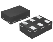
封装信息:
74LVC1G58提供了多种封装选项,例如SC-88、TSOP6、XSON6等,以适应不同的应用需求和空间限制。