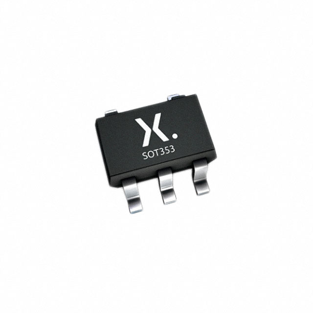
74LVC1G38-Q100
2-input NAND gate; open drain
Rev. 2 — 9 December 2016
Product data sheet
1. General description
The 74LVC1G38-Q100 provides a 2-input NAND function.
Inputs can be driven from either 3.3 V or 5 V devices. This feature allows the use of this
device as translator in a mixed 3.3 V and 5 V environment.
This device is fully specified for partial power-down applications using IOFF. The IOFF
circuitry disables the output, preventing the damaging backflow current through the device
when it is powered down.
This product has been qualified to the Automotive Electronics Council (AEC) standard
Q100 (Grade 1) and is suitable for use in automotive applications.
2. Features and benefits
Automotive product qualification in accordance with AEC-Q100 (Grade 1)
Specified from 40 C to +85 C and from 40 C to +125 C
Wide supply voltage range from 1.65 V to 5.5 V
5 V tolerant outputs for interfacing with 5 V logic
High noise immunity
Complies with JEDEC standard:
JESD8-7 (1.65 V to 1.95 V)
JESD8-5 (2.3 V to 2.7 V)
JESD8-B/JESD36 (2.7 V to 3.6 V).
24 mA output drive (VCC = 3.0 V)
CMOS low power consumption
Open drain outputs
Latch-up performance exceeds 250 mA
Direct interface with TTL levels
Inputs accept voltages up to 5 V
ESD protection:
MIL-STD-883, method 3015 exceeds 2000 V
HBM JESD22-A114F exceeds 2000 V
MM JESD22-A115-A exceeds 200 V (C = 200 pF, R = 0 )
�74LVC1G38-Q100
Nexperia
2-input NAND gate; open drain
3. Ordering information
Table 1.
Ordering information
Type number
Package
Temperature range Name
Description
Version
74LVC1G38GW-Q100
40 C to +125 C
TSSOP5
plastic thin shrink small outline package; 5 leads;
body width 1.25 mm
SOT353-1
74LVC1G38GV-Q100
40 C to +125 C
SC-74A
plastic surface-mounted package; 5 leads
SOT753
4. Marking
Table 2.
Marking
Type number
Marking code[1]
74LVC1G38GW-Q100
YB
74LVC1G38GV-Q100
YB
[1]
The pin 1 indicator is located on the lower left corner of the device, below the marking code.
5. Functional diagram
<
�
$
�
< �
�
%
�
�
Logic symbol
%
*1'
���DDE���
���DDE���
Fig 1.
$
Fig 2.
���DDE���
IEC logic symbol
Fig 3.
Logic diagram
6. Pinning information
6.1 Pinning
��/9&�*���4���
$
�
%
�
*1'
�
�
9&&
�
<
DDD�������
Fig 4.
Pin configuration for SOT353-1 and SOT753
74LVC1G38_Q100
Product data sheet
All information provided in this document is subject to legal disclaimers.
Rev. 2 — 9 December 2016
©
Nexperia B.V. 2017. All rights reserved
2 of 13
�74LVC1G38-Q100
Nexperia
2-input NAND gate; open drain
6.2 Pin description
Table 3.
Pin description
Symbol
Pin
Description
A
1
data input
B
2
data input
GND
3
ground (0 V)
Y
4
data output
VCC
5
supply voltage
7. Functional description
Table 4.
Function table[1]
Input
Output
A
B
L
L
Z
L
H
Z
H
L
Z
H
H
L
[1]
Y
H = HIGH voltage level; L = LOW voltage level; Z = high-impedance OFF state.
8. Limiting values
Table 5.
Limiting values
In accordance with the Absolute Maximum Rating System (IEC 60134). Voltages are referenced to GND (ground = 0 V).
Symbol
Parameter
VCC
supply voltage
IIK
input clamping current
Conditions
Min
Max
Unit
0.5
+6.5
V
50
-
[1]
0.5
+6.5
VI < 0 V
mA
VI
input voltage
IOK
output clamping current
VO > VCC or VO < 0 V
-
50
mA
VO
output voltage
Active mode
[1][2]
0.5
+6.5
V
Power-down mode
[1][2]
0.5
+6.5
V
-
50
mA
IO
output current
ICC
supply current
-
100
mA
IGND
ground current
100
-
mA
Tstg
storage temperature
65
+150
C
-
300
mW
total power dissipation
Ptot
VO = 0 V to VCC
V
Tamb = 40 C to +125 C
[3]
[1]
The input and output voltage ratings may be exceeded if the input and output current ratings are observed.
[2]
When VCC = 0 V (Power-down mode), the output voltage can be 5.5 V in normal operation.
[3]
For TSSOP5 and SC-74A packages: above 87.5 C the value of Ptot derates linearly with 4.0 mW/K.
74LVC1G38_Q100
Product data sheet
All information provided in this document is subject to legal disclaimers.
Rev. 2 — 9 December 2016
©
Nexperia B.V. 2017. All rights reserved
3 of 13
�74LVC1G38-Q100
Nexperia
2-input NAND gate; open drain
9. Recommended operating conditions
Table 6.
Recommended operating conditions
Symbol
Parameter
VCC
supply voltage
VI
input voltage
VO
output voltage
Conditions
Min
Typ
Max
Unit
1.65
-
5.5
V
0
-
5.5
V
Active mode
0
-
5.5
V
Disable mode; VCC = 1.65 V to 5.5 V
0
-
5.5
V
Power-down mode; VCC = 0 V
0
-
5.5
V
40
-
+125
C
-
-
20
ns/V
-
-
10
ns/V
Min
Typ
Tamb
ambient temperature
t/V
input transition rise and VCC = 1.65 V to 2.7 V
fall rate
VCC = 2.7 V to 5.5 V
10. Static characteristics
Table 7.
Static characteristics
At recommended operating conditions; voltages are referenced to GND (ground = 0 V).
Symbol Parameter
Tamb = 40 C to +85
VIH
VIL
VOL
Conditions
Max
Unit
C[1]
HIGH-level input voltage
LOW-level input voltage
LOW-level output voltage
VCC = 1.65 V to 1.95 V
0.65VCC
-
-
V
VCC = 2.3 V to 2.7 V
1.7
-
-
V
VCC = 2.7 V to 3.6 V
2.0
-
-
V
VCC = 4.5 V to 5.5 V
0.7VCC
-
-
V
VCC = 1.65 V to 1.95 V
-
-
0.35VCC
V
VCC = 2.3 V to 2.7 V
-
-
0.7
V
VCC = 2.7 V to 3.6 V
-
-
0.8
V
VCC = 4.5 V to 5.5 V
-
-
0.3VCC
V
VI = VIH or VIL
-
-
-
IO = 100 A; VCC = 1.65 V to 5.5 V
-
-
0.1
V
IO = 4 mA; VCC = 1.65 V
-
-
0.45
V
IO = 8 mA; VCC = 2.3 V
-
-
0.3
V
IO = 12 mA; VCC = 2.7 V
-
-
0.4
V
IO = 24 mA; VCC = 3.0 V
-
-
0.55
V
IO = 32 mA; VCC = 4.5 V
-
-
0.55
V
II
input leakage current
VI = 5.5 V or GND;
VCC = 0 V to 5.5 V
-
0.1
1
A
IOZ
OFF-state output current
VI = VIH or VIL; VO = VCC or GND;
VCC = 5.5 V
-
0.1
2
A
IOFF
power-off leakage current VI or VO = 5.5 V; VCC = 0 V
-
0.1
2
A
ICC
supply current
VI = 5.5 V or GND;
VCC = 1.65 V to 5.5 V; IO = 0 A
-
0.1
4
A
ICC
additional supply current
VI = VCC 0.6 V; IO = 0 A;
VCC = 2.3 V to 5.5 V; per pin
-
5
500
A
CI
input capacitance
-
2.5
-
pF
74LVC1G38_Q100
Product data sheet
All information provided in this document is subject to legal disclaimers.
Rev. 2 — 9 December 2016
©
Nexperia B.V. 2017. All rights reserved
4 of 13
�74LVC1G38-Q100
Nexperia
2-input NAND gate; open drain
Table 7.
Static characteristics …continued
At recommended operating conditions; voltages are referenced to GND (ground = 0 V).
Symbol Parameter
Conditions
Min
Typ
Max
Unit
0.65VCC
-
-
V
Tamb = 40 C to +125 C
HIGH-level input voltage
VIH
LOW-level input voltage
VIL
LOW-level output voltage
VOL
VCC = 1.65 V to 1.95 V
VCC = 2.3 V to 2.7 V
1.7
-
-
V
VCC = 2.7 V to 3.6 V
2.0
-
-
V
VCC = 4.5 V to 5.5 V
0.7VCC
-
-
V
VCC = 1.65 V to 1.95 V
-
-
0.35VCC
V
VCC = 2.3 V to 2.7 V
-
-
0.7
V
VCC = 2.7 V to 3.6 V
-
-
0.8
V
VCC = 4.5 V to 5.5 V
-
-
0.3VCC
V
VI = VIH or VIL
-
-
-
IO = 100 A; VCC = 1.65 V to 5.5 V
-
-
0.1
V
IO = 4 mA; VCC = 1.65 V
-
-
0.70
V
IO = 8 mA; VCC = 2.3 V
-
-
0.45
V
IO = 12 mA; VCC = 2.7 V
-
-
0.60
V
IO = 24 mA; VCC = 3.0 V
-
-
0.80
V
IO = 32 mA; VCC = 4.5 V
-
-
0.80
V
II
input leakage current
VI = 5.5 V or GND;
VCC = 0 V to 5.5 V
-
-
1
A
IOZ
OFF-state output current
VI = VIH or VIL; VO = VCC or GND;
VCC = 5.5 V
-
-
2
A
IOFF
power-off leakage current VI or VO = 5.5 V; VCC = 0 V
-
-
2
A
ICC
supply current
VI = 5.5 V or GND;
VCC = 1.65 V to 5.5 V; IO = 0 A
-
-
4
A
ICC
additional supply current
VI = VCC 0.6 V; IO = 0 A;
VCC = 2.3 V to 5.5 V; per pin
-
-
500
A
[1]
All typical values are measured at VCC = 3.3 V and Tamb = 25 C.
74LVC1G38_Q100
Product data sheet
All information provided in this document is subject to legal disclaimers.
Rev. 2 — 9 December 2016
©
Nexperia B.V. 2017. All rights reserved
5 of 13
�74LVC1G38-Q100
Nexperia
2-input NAND gate; open drain
11. Dynamic characteristics
Table 8.
Dynamic characteristics
Voltages are referenced to GND (ground = 0 V); for test circuit see Figure 6.
Symbol Parameter
propagation delay
tpd
power dissipation
capacitance
CPD
40 C to +85 C
Conditions
40 C to +125 C
Unit
Min
Typ[1]
Max
Min
Max
VCC = 1.65 V to 1.95 V
1.0
3.0
10.0
1.0
12.5
ns
VCC = 2.3 V to 2.7 V
0.5
1.8
6.0
0.5
7.5
ns
VCC = 2.7 V
0.5
2.5
5.0
0.5
6.5
ns
VCC = 3.0 V to 3.6 V
0.5
2.3
4.5
0.5
5.7
ns
VCC = 4.5 V to 5.5 V
0.5
1.5
3.9
0.5
4.9
ns
-
6
-
-
-
pF
A, B to Y; see Figure 5
[2]
[3]
VCC = 3.3 V;
VI = GND to VCC
[1]
Typical values are measured at Tamb = 25 C and VCC = 1.8 V, 2.5 V, 2.7 V, 3.3 V and 5.0 V respectively.
[2]
tpd is the same as tPZL and tPLZ.
[3]
CPD is used to determine the dynamic power dissipation (PD in W).
PD = CPD VCC2 fi N + (CL VCC2 fo) where:
fi = input frequency in MHz;
fo = output frequency in MHz;
CL = output load capacitance in pF;
VCC = supply voltage in V;
N = number of inputs switching;
(CL VCC2 fo) = sum of outputs.
12. Waveform and test circuit
9,
$��%�LQSXW
90
*1'
W 3/=
W 3=/
9&&
很抱歉,暂时无法提供与“74LVC1G38GW-Q100H”相匹配的价格&库存,您可以联系我们找货
免费人工找货- 国内价格 香港价格
- 3000+0.570333000+0.07387
- 6000+0.551416000+0.07142
- 9000+0.541949000+0.07019
- 15000+0.5314415000+0.06883
- 21000+0.5253121000+0.06804
- 30000+0.5194030000+0.06727
- 国内价格
- 5+0.98216
- 50+0.96012
- 150+0.94544
- 国内价格 香港价格
- 1+1.506331+0.19509
- 10+0.9892710+0.12812
- 25+0.8730325+0.11307
- 100+0.74120100+0.09600
- 250+0.67813250+0.08783
- 500+0.64033500+0.08293
- 1000+0.608971000+0.07887