74AHC138-Q100;
74AHCT138-Q100
3-to-8 line decoder/demultiplexer; inverting
Rev. 2 — 2 April 2014
Product data sheet
1. General description
The 74AHC138-Q100; 74AHCT138-Q100 are high-speed Si-gate CMOS devices and are
pin compatible with Low-power Schottky TTL (LSTTL). They are specified in compliance
with JEDEC standard No. 7A.
The 74AHC138-Q100; 74AHCT138-Q100 is a 3-to-8 line decoder/demultiplexer. It
accepts three binary weighted address inputs (A0, A1 and A2). When enabled, it
provides eight mutually exclusive outputs (Y0 to Y7) that are LOW when selected. There
are three enable inputs: two active LOW (E1 and E2) and one active HIGH (E3). Every
output is HIGH unless E1 and E2 are LOW and E3 is HIGH.
This multiple enable function, allows easy parallel expansion of the device to a 1-of-32
(5 lines to 32 lines) decoder with just four 74AHC138-Q100; 74AHCT138-Q100 devices
and one inverter. The 74AHC138-Q100; 74AHCT138-Q100 can be used as an eight
output demultiplexer by using one of the active LOW enable inputs as the data input and
the remaining enable inputs as strobes. Unused enable inputs must be permanently tied
to their appropriate active HIGH or LOW state.
This product has been qualified to the Automotive Electronics Council (AEC) standard
Q100 (Grade 1) and is suitable for use in automotive applications.
2. Features and benefits
Automotive product qualification in accordance with AEC-Q100 (Grade 1)
Specified from 40 C to +85 C and from 40 C to +125 C
Balanced propagation delays
All inputs have Schmitt-trigger action
Demultiplexing capability
Multiple input enable for easy expansion
Ideal for memory chip select decoding
Inputs accept voltages higher than VCC
For 74AHC138-Q100 only: operates with CMOS input levels
For 74AHCT138-Q100 only: operates with TTL input levels
ESD protection:
MIL-STD-883, method 3015 exceeds 2000 V
HBM JESD22-A114F exceeds 2000 V
MM JESD22-A115-A exceeds 200 V (C = 200 pF, R = 0 )
Multiple package options
�74AHC138-Q100; 74AHCT138-Q100
Nexperia
3-to-8 line decoder/demultiplexer; inverting
3. Ordering information
Table 1.
Ordering information
Type number
Package
74AHC138D-Q100
Temperature range
Name
Description
Version
40 C to +125 C
SO16
plastic small outline package; 16 leads;
body width 3.9 mm
SOT109-1
40 C to +125 C
TSSOP16
plastic thin shrink small outline package; 16
leads; body width 4.4 mm
SOT403-1
40 C to +125 C
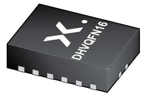
DHVQFN16 plastic dual in-line compatible thermal-enhanced SOT763-1
very thin quad flat package; no leads; 16
terminals; body 2.5 3.5 0.85 mm
74AHCT138D-Q100
74AHC138PW-Q100
74AHCT138PW-Q100
74AHC138BQ-Q100
74AHCT138BQ-Q100
4. Functional diagram
DX
1
A0
1
Y0
A1
Y1
14
3
A2
Y2
13
Y3
12
E1
Y4
11
E2
Y5
10
E3
Y6
9
Y7
7
4
5
6
3
G
0
7
2
2
3
4
4
&
5
5
6
6
7
14
1
13
2
12
3
1
1
2
2
4
3
11
4
10
4
9
5
7
0
&
5
6
EN
6
7
15
14
13
12
11
10
9
7
mna371
Logic symbol
Fig 2.
(b)
IEC logic symbol
Y0
15
1
A0
Y1
14
2
A1
Y2
13
3
A2
Y3
12
Y4
11
Y5
10
Y6
9
Y7
7
3-to-8
DECODER
4
X/Y
15
(a)
mna370
Fig 1.
1
2
15
2
0
0
ENABLE
EXITING
E1
5
E2
6
E3
mna372
Fig 3.
Functional diagram
74AHC_AHCT138_Q100
Product data sheet
All information provided in this document is subject to legal disclaimers.
Rev. 2 — 2 April 2014
©
Nexperia B.V. 2017. All rights reserved
2 of 17
�74AHC138-Q100; 74AHCT138-Q100
Nexperia
3-to-8 line decoder/demultiplexer; inverting
5. Pinning information
5.1 Pinning
��$+&����4���
��$+&7����4���
$�
WHUPLQDO��
LQGH[�DUHD
�� 9&&
��$+&����4���
��$+&7����4���
�
�� 9&&
$�
�
��
很抱歉,暂时无法提供与“74AHC138D-Q100J”相匹配的价格&库存,您可以联系我们找货
免费人工找货- 国内价格 香港价格
- 1+3.182981+0.41231
- 10+2.2174110+0.28724
- 25+1.9751625+0.25586
- 100+1.70386100+0.22071
- 250+1.57509250+0.20403
- 500+1.49752500+0.19398
- 1000+1.433481000+0.18569
- 国内价格
- 1+1.06262
- 10+0.83906
- 30+0.74326
- 100+0.62370
- 500+0.57046
- 1000+0.53849
- 国内价格 香港价格
- 2500+1.206602500+0.15630
- 5000+1.169825000+0.15154
- 7500+1.151417500+0.14915
- 12500+1.1310112500+0.14651
- 17500+1.1190817500+0.14496
- 25000+1.1076225000+0.14348