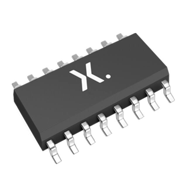
74HC42
BCD to decimal decoder (1-of-10)
Rev. 3 — 27 September 2016
Product data sheet
1. General description
The 74HC42 is a one of ten BCD to decimal decoder. It accepts four BCD inputs (0A to
3A) and provides ten mutually exclusive outputs (0Y to 9Y). The logic design ensures that
all outputs are HIGH when binary codes greater than nine are applied to the inputs. The
most significant input (3A) produces an useful inhibit function when the device is used as
a 1-of-8 decoder. The 3A input can also be used as the data input in an 8-output
demultiplexer application. Inputs include clamp diodes. This enables the use of current
limiting resistors to interface inputs to voltages in excess of VCC.
2. Features and benefits
Complies with JEDEC standard no. 7A
Input levels:
For 74HC42: CMOS level
Mutually exclusive outputs
1-of-8 demultiplexing capability
Outputs disabled for input codes above nine
ESD protection:
HBM JESD22-A114F exceeds 2000 V
MM JESD22-A115-A exceeds 200 V
Specified from 40 C to +85 C and 40 C to +125 C
3. Ordering information
Table 1.
Ordering information
Type number Temperature range
74HC42D
40 C to +125 C
Name
Description
Version
SO16
plastic small outline package; 16 leads; body width 3.9 mm SOT109-1
�74HC42
Nexperia
BCD to decimal decoder (1-of-10)
4. Functional diagram
�<
�<
�<
�<
�<
�<
�<
�<
�<
�<
%&'�'(&
��
�$
��
�$
��
�$
��
�$
�<
�<
�<
�<
�<
�<
�<
�<
�<
�<
�
�
�
�
�
�
�
�
��
��
��
��
��
��
DDD�������
Fig 1.
Logic symbol
�
�
�
�
�
�
�
�
�
�
�
�
�
�
�
�
�
�
�
�
�
�
��
��
�$
��
�$
��
�$
��
�$
��
DDD�������
DDD�������
Fig 2.
IEC logic symbol
�
�
�
�
�
�
�
�
��
��
Fig 3.
Functional diagram
�<
�<
�$
�<
�<
�<
�$
�<
�<
�$
�<
�<
�$
�<
DDD�������
Fig 4.
Logic diagram
74HC42
Product data sheet
All information provided in this document is subject to legal disclaimers.
Rev. 3 — 27 September 2016
©
Nexperia B.V. 2017. All rights reserved
2 of 12
�74HC42
Nexperia
BCD to decimal decoder (1-of-10)
5. Pinning information
5.1 Pinning
��+&��
�<
�
�� 9&&
�<
�
�� �$
�<
�
�� �$
�<
�
�� �$
�<
�
�� �$
�<
�
�� �<
�<
�
�� �<
*1'
�
�
�<
DDD�������
Fig 5.
Pin configuration
5.2 Pin description
Table 2.
Pin description
Symbol
Pin
Description
0Y, 1Y, 2Y, 3Y, 4Y, 5Y, 6Y, 7Y, 8Y, 9Y
1, 2, 3, 4, 5, 6, 7, 9, 10, 11
multiplexer output
GND
8
ground (0 V)
0A, 1A, 2A, 3A
15, 14, 13, 12
data input
VCC
16
supply voltage
74HC42
Product data sheet
All information provided in this document is subject to legal disclaimers.
Rev. 3 — 27 September 2016
©
Nexperia B.V. 2017. All rights reserved
3 of 12
�74HC42
Nexperia
BCD to decimal decoder (1-of-10)
6. Functional description
Function table[1]
Table 3.
Inputs
Outputs
3A
2A
1A
0A
0Y
1Y
2Y
3Y
4Y
5Y
6Y
7Y
8Y
9Y
L
L
L
L
L
H
H
H
H
H
H
H
H
H
L
L
L
H
H
L
H
H
H
H
H
H
H
H
L
L
H
L
H
H
L
H
H
H
H
H
H
H
L
L
H
H
H
H
H
L
H
H
H
H
H
H
L
H
L
L
H
H
H
H
L
H
H
H
H
H
L
H
L
H
H
H
H
H
H
L
H
H
H
H
L
H
H
L
H
H
H
H
H
H
L
H
H
H
L
H
H
H
H
H
H
H
H
H
H
L
H
H
H
L
L
L
H
H
H
H
H
H
H
H
L
H
H
L
L
H
H
H
H
H
H
H
H
H
H
L
H
L
H
L
H
H
H
H
H
H
H
H
H
H
H
L
H
H
H
H
H
H
H
H
H
H
H
H
H
H
L
L
H
H
H
H
H
H
H
H
H
H
H
H
L
H
H
H
H
H
H
H
H
H
H
H
H
H
H
L
H
H
H
H
H
H
H
H
H
H
H
H
H
H
H
H
H
H
H
H
H
H
H
H
[1]
H = HIGH voltage level;
L = LOW voltage level
7. Limiting values
Table 4.
Limiting values
In accordance with the Absolute Maximum Rating System (IEC 60134). Voltages are referenced to GND (ground = 0 V).
Symbol
Parameter
Conditions
Min
Max
Unit
VCC
supply voltage
0.5
+7
V
IIK
input clamping current
VI < 0.5 V or VI > VCC + 0.5 V
[1]
-
20
mA
IOK
output clamping current
VO < 0.5 V or VO > VCC + 0.5 V
[1]
-
20
mA
IO
output current
0.5 V < VO < VCC + 0.5 V
-
25
mA
ICC
supply current
-
50
mA
IGND
ground current
50
-
mA
Tstg
storage temperature
65
+150
C
-
500
mW
[2]
total power dissipation
Ptot
[1]
The input and output voltage ratings may be exceeded if the input and output current ratings are observed.
[2]
For SO16 package: Ptot derates linearly with 8 mW/K above 70 C.
74HC42
Product data sheet
All information provided in this document is subject to legal disclaimers.
Rev. 3 — 27 September 2016
©
Nexperia B.V. 2017. All rights reserved
4 of 12
�74HC42
Nexperia
BCD to decimal decoder (1-of-10)
8. Recommended operating conditions
Table 5.
Recommended operating conditions
Voltages are referenced to GND (ground = 0 V)
Symbol
Parameter
Conditions
74HC42
Min
Typ
Unit
Max
VCC
supply voltage
2.0
5.0
6.0
V
VI
input voltage
0
-
VCC
V
VO
output voltage
0
-
VCC
V
Tamb
ambient temperature
40
+25
+125
C
t/V
input transition rise and fall rate
VCC = 2.0 V
-
-
625
ns/V
VCC = 4.5 V
-
1.67
139
ns/V
VCC = 6.0 V
-
-
83
ns/V
9. Static characteristics
Table 6.
Static characteristics
At recommended operating conditions; voltages are referenced to GND (ground = 0 V).
Symbol Parameter
VIH
VIL
VOH
VOL
HIGH-level
input voltage
LOW-level
input voltage
25 C
Conditions
40 C to +85 C
40 C to +125 C
Unit
Min
Typ
Max
Min
Max
Min
Max
VCC = 2.0 V
1.5
1.2
-
1.5
-
1.5
-
V
VCC = 4.5 V
3.15
2.4
-
3.15
-
3.15
-
V
VCC = 6.0 V
4.2
3.2
-
4.2
-
4.2
-
V
VCC = 2.0 V
-
0.8
0.5
-
0.5
-
0.5
V
VCC = 4.5 V
-
2.1
1.35
-
1.35
-
1.35
V
VCC = 6.0 V
-
2.8
1.8
-
1.8
-
1.8
V
HIGH-level
VI = VIH or VIL
output voltage
IO = 20 A; VCC = 2.0 V
1.9
2.0
-
1.9
-
1.9
-
V
IO = 20 A; VCC = 4.5 V
4.4
4.5
-
4.4
-
4.4
-
V
IO = 20 A; VCC = 6.0 V
5.9
6.0
-
5.9
-
5.9
-
V
IO = 4.0 mA; VCC = 4.5 V
3.98 4.32
-
3.84
-
3.7
-
V
IO = 5.2 mA; VCC = 6.0 V
5.48 5.81
-
5.34
-
5.2
-
V
LOW-level
VI = VIH or VIL
output voltage
IO = 20 A; VCC = 2.0 V
-
0
0.1
-
0.1
-
0.1
V
IO = 20 A; VCC = 4.5 V
-
0
0.1
-
0.1
-
0.1
V
IO = 20 A; VCC = 6.0 V
-
0
0.1
-
0.1
-
0.1
V
IO = 4.0 mA; VCC = 4.5 V
-
0.15
0.26
-
0.33
-
0.4
V
IO = 5.2 mA; VCC = 6.0 V
-
0.16
0.26
-
0.33
-
0.4
V
VI = VCC or GND; VCC = 6.0 V
-
-
0.1
-
1.0
-
1.0
A
II
input leakage
current
ICC
supply current VI = VCC or GND; IO = 0 A;
VCC = 6.0 V
-
-
8.0
-
80
-
160
A
CI
input
capacitance
-
3.5
-
-
-
-
-
pF
74HC42
Product data sheet
All information provided in this document is subject to legal disclaimers.
Rev. 3 — 27 September 2016
©
Nexperia B.V. 2017. All rights reserved
5 of 12
�74HC42
Nexperia
BCD to decimal decoder (1-of-10)
10. Dynamic characteristics
Table 7.
Dynamic characteristics
Voltages are referenced to GND (ground = 0 V); CL = 50 pF unless otherwise specified; for test circuit see Figure 7.
Symbol Parameter
25 C
Conditions
Min
Typ
Max
Min
Max
Min
Max
-
47
150
-
190
-
225
ns
VCC = 4.5 V
-
17
30
-
38
-
45
ns
VCC = 5.0 V; CL = 15 pF
-
17
-
-
-
-
-
ns
-
14
26
-
33
-
38
ns
VCC = 2.0 V
-
19
75
-
95
-
110
ns
VCC = 4.5 V
-
7
15
-
19
-
22
ns
-
6
13
-
16
-
19
ns
-
37
-
-
-
-
-
pF
[1]
propagation nA to nY; see Figure 6
delay
VCC = 2.0 V
tpd
VCC = 6.0 V
transition
time
tt
[2]
see Figure 6
VCC = 6.0 V
[3]
power
per package; VI = GND to VCC
dissipation
capacitance
CPD
40 C to +85 C 40 C to +125 C Unit
[1]
tpd is the same as tPHL and tPLH.
[2]
tt is the same as tTHL and tTLH.
[3]
CPD is used to determine the dynamic power dissipation (PD in W):
PD = CPD VCC2 fi N + (CL VCC2 fo) where:
fi = input frequency in MHz;
fo = output frequency in MHz;
CL = output load capacitance in pF;
VCC = supply voltage in V;
N = number of inputs switching;
(CL VCC2 fo) = sum of outputs.
11. Waveforms
9,
Q$�LQSXW
90
*1'
92+
W3+/
90
9;
Q
很抱歉,暂时无法提供与“74HC42D,653”相匹配的价格&库存,您可以联系我们找货
免费人工找货- 国内价格
- 1+9.76320
- 10+8.15400
- 30+7.26840
- 100+6.27480
- 500+5.82120
- 1000+5.62680
- 国内价格
- 1+9.60097
- 10+6.99732
- 100+6.02095
- 国内价格 香港价格
- 1+6.094971+0.78918
- 10+4.2985010+0.55657
- 25+3.8559525+0.49927
- 100+3.37124100+0.43651
- 250+3.14048250+0.40663
- 500+3.00120500+0.38860
- 1000+2.952471000+0.38229
- 国内价格 香港价格
- 2500+2.765822500+0.35812
- 5000+2.692925000+0.34868
- 7500+2.656427500+0.34396
- 12500+2.6159912500+0.33872
- 17500+2.5923517500+0.33566
- 25000+2.5696125000+0.33272