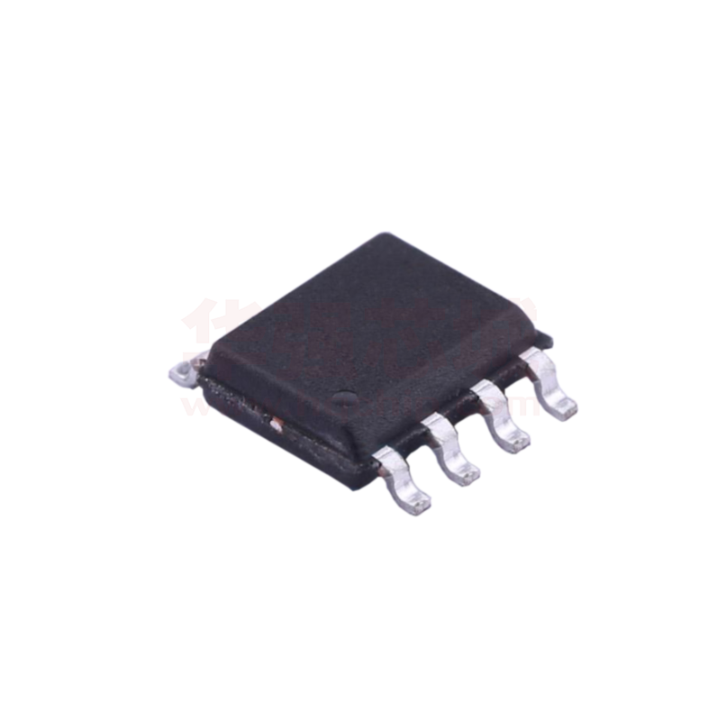
LMC555
CMOS general purpose timer
The LMC555 is CMOS RC timers providing significantly improved
performance over the standard SE/NE555 and 355 timers, while at
the same time being direct replacements for those devices in most
applications. Improved parameters include low supply current, wide
operating supply voltage range, low THRESHOLD, TRIGGER and
RESET currents, no crowbarring of the supply current during output
transitions, higher frequency performance and no requirement to
decouple CONTROL VOLTAGE for stable operation.
Specifically, the LMC555 is stable controller capable of producing
accurate time delays of frequencies.
•
•
•
•
•
•
•
•
8
1
ORDERING INFORMATION
ILC555N Plastic
IZC555 Chip
TA = -20° to 70° C for
the package
Exact equivalent in most cases for SE/NE555.
Low Supply Current.
High speed operation – 500 kHz guaranteed.
Wide operation supply voltage range – 2 to 18 volts.
Timing from microseconds through hours.
Operates in both astable and monostable modes.
Adjustable duty cycle.
High output source/sink driver can drive TTL/CMOS
http://www.hgsemi.com.cn
N SUFFIX
PLASTIC
PIN ASSIGNMENT
1
GND
01
08
TRIGGER
02
07 DISCHARGE
OUTPUT
03
06 THRESHOLD
RESET
04
05
LMC555
VCC
CONTROL
VOLTAGE
2018 JUN
�LMC555
TRUTH TABLE
THRESHOLD
TRIGGER
RESET
OUTPUT
DISCHARGE
X
X
L
L
ON
> 2/3⋅VCC
> 1/3⋅VCC
H
L
ON
< 2/3⋅VCC
> 1/3⋅VCC
H
STABLE
STABLE
X
< 1/3⋅VCC
H
H
OFF
MAXIMUM RATINGS AND RECOMMENDED OPERATING CONDITIONS
Parameter, unit
Symbol
Recommended operating
conditions
Maximum ratings
Value
Value
min
max
min
max
2.0
18.0
0
18.0
IO
-
20
-
100
VTH, VTRIG, VRST
-
-
-0.3
VCC+0.3
Power Dissipation, mW
PD
-
-
-
200
Operating Temperature,°С
TOPR
-20
70
-20
85
Storage Temperature, °С
TSTG
-
-
-65
150
Lead Temperature, 1 mm from
Case for 10 Seconds, °С
TSOLDER
-
-
Supply Voltage, V
Output Current, mА
Input Voltage, V
http://www.hgsemi.com.cn
VCC
2
260
2018 JUN
�LMC555
DC ELECTRICAL CHARACTERISTICS (Voltages Referenced to GND)
Parameter, units
Symbol
Test Conditions
IOL, IOH
Threshold Voltage, V
Trigger voltage, V
VTH
VCC, В
5.0
VTRIG
5.0
2.0
Reset voltage, V
VRST
Value
Temperature, °С
min
max
0.65 VCC
0.70 VCC
25±10
0.60 VCC
0.80 VCC
-20, 70
0.31 VCC
0.36 VCC
25±10
0.28 VCC
0.40 VCC
-20, 70
0.4
1.0
25±10
0.2
1.5
-20, 70
0.65 VCC
0.69 VCC
25±10
0.60 VCC
0.80 VCC
-20, 70
25±10
18.0
2.0
18.0
Control Voltage Lead, V
Output voltage Low, V
Output voltage High, V
VCV
VOL
IOL = 3.2 mА
5.0
0.4
IOL = 20 mА
15.0
1.0
IOL = 3.2 mА
5.0
0.6
IOL = 20 mА
15.0
1.5
VOH
IOH = -0.8 mА
Supply Current, μA
http://www.hgsemi.com.cn
ICC
3
5.0
4.0
15.0
14.3
5.0
3.5
15.0
14.0
-20, 70
25±10
-20, 70
2.0
200
18.0
300
2.0
400
18.0
600
25±10
-20, 70
2018 JUN
�LMC555
AC ELECTRICAL CHARACTERISTICS
Parameter, unit
Symbol
Test Conditions
Value
RL, CL
VCC,
V
Rise (Fall) Time of Output,
ns
tTHL, tTLH RL = 10 МΩ, CL = 10 pF
Guaranteed Max Osc Freq,
kHz
fMAX
Initial accuracy, %
Drift with Temperature,
%/°С
5.0
Astable Operation
2.018.0
αf
RL = 1 - 100 kΩ,
CL = 0.1 μF
Drift with Supply Voltage,
%/В
Δf
Min
Max
Temperature,
°С
35
75
25±10
70
500
150
-20, 70
25±10
200
5
-20, 70
5.0
0.02
-20, 70
10.0
15.0
5.0
0.03
0.06
3
6
25±10
-20, 70
TRIGGER
COMPARATOR A
THRESHOLD
COMPARATOR B
Figura 1. Block Diagram
VCC
0.9
TRIGGER
GND
0.1
tHL
VCC
0.9
0.9
OUTPUT
0.1
0.1
tTLH
GND
tTHL
Figura 2. Switcing Waveforms
http://www.hgsemi.com.cn
4
2018 JUN
�
