HTC721, HTC722, HTC724
12MHz, High Slew Rate, RRIO CMOS Operational Amplifiers
General Description
The HTC721 (single), HTC722 (dual) and HTC724 (quad) are low noise, Low voltage and
high slew rate operational amplifiers with an excellent bandwidth of 12MHz, a slew rate of
7 V/μs, and a quiescent current of 820μA per amplifier at 5V, the HTC72x family can be
designed into a wide range of applications.
The HTC72x op-amps are designed to provide optimal performance in low voltage and
low noise systems The input common-mode voltage range includes ground, and the
maximum input offset voltage are 4.0mV. These parts provide rail-to-rail output swing into
heavy loads. The HTC72x family is specified for single or dual power supplies of +2.3V to
+5.5V. All models are specified over the extended industrial temperature range of −40℃
to +125℃.
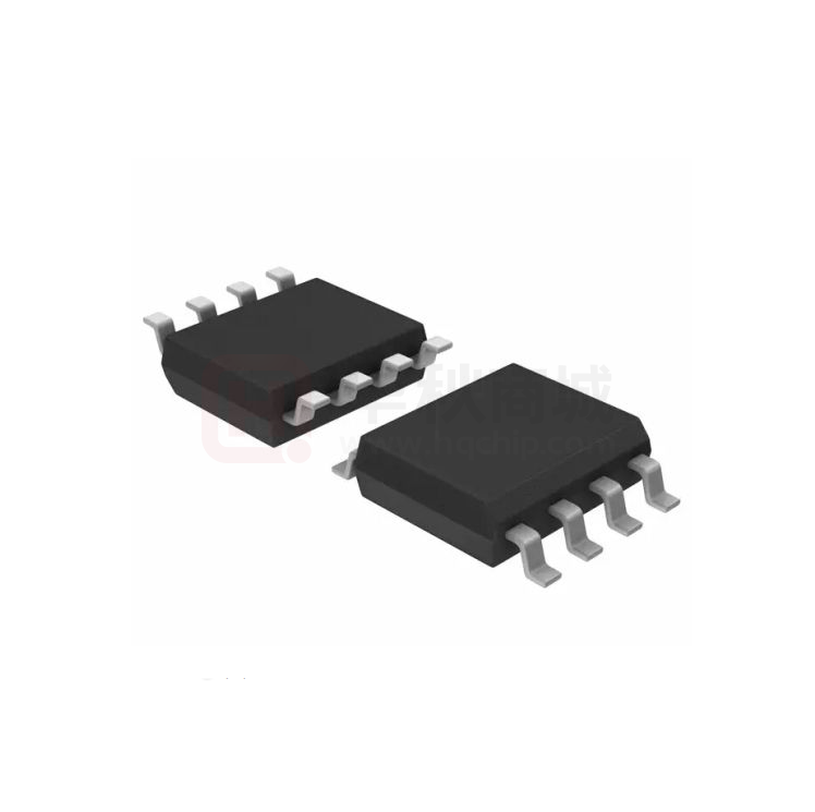
The HTC721 is available in 5-lead SC70 and SOT-23 packages. The HTC722 is available
in 8-lead MSOP and SOIC packages. The HTC724 is available in 14-lead TSSOP and
SOIC packages.
Features and Benefits
High Slew Rate: 7 V/μs
Wide Bandwidth: 12 MHz
Low Power: 820 μA per Amplifier Supply Current
Settling Time to 0.1% with 2V Step: 0.26 μs
Overload Recovery Time: 0.31 μs
Low Noise : 45 nV/√Hz
High Gains of 110 dB for Active Filters and Gain Stages
Low Offset Voltage: 4.2 mV Maximum
Unit Gain Stable
Rail-to-Rail Input and Output
– Input Voltage Range: -0.2 to +5.2 V at 5V Supply
Operating Power Supply: +2.3 V to +5.5 V
Operating Temperature Range: −40℃ to +125℃
Applications
Photodiode Amplification
Sensor Interfaces
Audio Outputs
Active Filters
Driving A/D Converters
Portable Equipment
Battery-Powered Instrumentation
Pin Configurations (Top View)
OUT
1
﹣VS
2
﹢IN
3
HTC721
HTC722
SC70/SOT23-5
DFN-8L 2*2
5
﹢VS
OUT A
﹣IN A
﹢IN A
4
﹣IN
﹣VS
1
2
3
4
8
7
6
5
﹢VS
OUT B
﹣IN B
﹢IN B
OUT A
﹣IN A
HTC722
HTC724
MSOP-8/SO-8
TSSOP-14/SO-14
8
1
2
﹢IN A
3
﹣VS
4
7
A
B
﹢VS
OUT B
6
﹣IN B
5
﹢IN B
OUT A
1
14
﹣IN A
2
13
﹣IN D
﹢IN A
3
12
﹢IN D
﹢VS
4
11
﹣VS
﹢IN B
5
10
﹢IN C
﹣IN B
6
9
﹣IN C
OUT B
7
8
OUT C
A
B
1
HUATECH
SEMICONDUCTOR
OUT D
D
C
CAUTION: These devices are sensitive to electrostatic discharge; follow proper IC Handling Procedures.
Huatech (and design) is a registered trademark of Huatech Semiconductor Inc.
Copyright Huatech Semiconductor Inc. All Rights Reserved.
All other trademarks mentioned are the property of their respective owners.
FN1615-36 (v.3.b)
�HTC721, HTC722, HTC724
12MHz, High Slew Rate, RRIO CMOS Operational Amplifiers
Pin Description
Symbol
Description
–IN
Inverting Input of the Amplifier. The Voltage range can go from (VS– – 0.2V) to (VS+ +
0.2V).
+IN
Non-Inverting Input of Amplifier. This pin has the same voltage range as –IN.
+VS
Positive Power Supply. The voltage is from 2.3V to 5.5V. Split supplies are possible as
long as the voltage between VS+ and VS– is between 2.3V and 5.5V. A bypass
capacitor of 0.1μF as close to the part as possible should be used between power
supply pins or between supply pins and ground.
–VS
Negative Power Supply. It is normally tied to ground. It can also be tied to a voltage
other than ground as long as the voltage between VS+ and VS– is from 2.3V to 5.5V. If it
is not connected to ground, bypass it with a capacitor of 0.1μF as close to the part as
possible.
OUT
Amplifier Output.
N/C
No Connection.
Ordering Information
Type Number
Package Name
Package Quantity
Marking Code
HTC721XC5/R6
SC70-5
Tape and Reel, 3 000
C71
HTC721XT5/R6
SOT23-5
Tape and Reel, 3 000
C71
HTC722XV8/R6
MSOP-8
Tape and Reel, 3 000
C72X
HTC722XS8/R8
SO-8
Tape and Reel, 4 000
C72X
HTC722XF8/R6
DFN-8L 2*2
Tape and Reel, 3 000
C72X
HTC724XT14/R6
TSSOP-14
Tape and Reel, 3 000
C74X
HTC724XS14/R5
SO-14
Tape and Reel, 2 500
C74X
Limiting Value
In accordance with the Absolute Maximum Rating System (IEC 60134).
Parameter
Absolute Maximum Rating
Supply Voltage, VS+ to VS–
7.0V
Common-Mode Input Voltage
VS– – 0.5V to VS+ + 0.5V
Storage Temperature Range
–65℃ to +150℃(TJ)
Junction Temperature
160℃
Lead Temperature Range (Soldering 10 sec)
260℃
HBM ±4 000V
Electrostatic Discharge Voltage
MM ±400V
NOTE 1: Stresses beyond those listed under Absolute Maximum Ratings may cause permanent damage to the device. These
are stress ratings only, which do not imply functional operation of the device at these or any other conditions beyond those
indicated under Recommended Operating Conditions. Exposure to absolute-maximum-rated conditions for extended periods
may affect device reliability.
NOTE 2: Provided device does not exceed maximum junction temperature (TJ) at any time.
2
HUATECH
SEMICONDUCTOR
CAUTION: These devices are sensitive to electrostatic discharge; follow proper IC Handling Procedures.
Huatech (and design) is a registered trademark of Huatech Semiconductor Inc.
Copyright Huatech Semiconductor Inc. All Rights Reserved.
All other trademarks mentioned are the property of their respective owners.
FN1615-36 (v.3.b)
�HTC721, HTC722, HTC724
12MHz, High Slew Rate, RRIO CMOS Operational Amplifiers
Electrical Characteristics
VS = 5.0V, TA = +25℃, VCM = VS /2, VO = VS /2, and RL = 10kΩ connected to VS /2, unless otherwise noted.
Boldface limits apply over the specified temperature range, TA = −40 to +125 ℃.
Symbol
Parameter
Conditions
Min.
Typ.
Max.
±0.5
+4.2
Unit
INPUT CHARACTERISTICS
VOS
Input offset voltage
-4.2
over Temperature
-4.5
VOS TC
Offset voltage drift
over Temperature
1
over Temperature
IOS
Input offset current
VCM
Common-mode voltage
range
Common-mode rejection
ratio
over Temperature
over Temperature
Open-loop voltage gain
AVOL
over Temperature
over Temperature
RIN
Input resistance
CIN
Input capacitance
800
1
VS––0.2
VCM = 0.05V to 3.0V
80
VCM = VS––0.1 to VS++0.1 V
RL = 10kΩ, VO = 0.05 to 3.5 V
RL = 600Ω, VO = 0.15 to 3.5 V
pA
pA
VS++0.2
V
94
70
60
mV
μV/℃
2
Input bias current
IB
CMRR
+4.5
dB
75
55
98
108
86
82
92
dB
72
GΩ
100
Differential
2.0
Common mode
3.5
pF
OUTPUT CHARACTERISTICS
VOH
High output voltage swing
VOL
Low output voltage swing
ZOUT
ISC
RL = 600Ω
VS+–100
RL = 10kΩ
VS+–8
RL = 600Ω
70
RL = 10kΩ
6
Closed-loop output
impedance
f = 200kHz, G = +1
0.4
Open-loop output
impedance
f = 1MHz, IO = 0
2.6
Source current through 10Ω
55
Sink current through 10Ω
50
Short-circuit current
mV
mV
Ω
mA
DYNAMIC PERFORMANCE
GBW
Gain bandwidth product
f = 1kHz
12
MHz
ΦM
Phase margin
CL = 100pF
66
°
SR
Slew rate
G = +1, CL = 100pF, VO = 1.5V to 3.5V
7
V/μs
BW P
Full power bandwidth
VS
THD+N
Total harmonic distortion +
f = 1kHz, G = +1, VO = 3VPP
noise
Min.
Typ.
Max.
Unit
0.31
μs
0.0013
%
NOISE PERFORMANCE
Vn
Input voltage noise
f = 0.1 to 10 Hz
8
μVP-P
en
Input voltage noise
density
f = 10kHz
45
nV/√Hz
POWER SUPPLY
VS
Operating supply voltage
PSRR
Power supply rejection
ratio
over Temperature
IQ
2.3
VS = 2.7V to 5.5V, VCM < VS+ − 2V
82
5.5
98
V
dB
75
Quiescent current (per
amplifier)
820
over Temperature
1050
μA
1250
THERMAL CHARACTERISTICS
TA
θJA
Operating temperature
range
Package Thermal
Resistance
4
-40
+125
SC70-5
333
SOT23-5
190
MSOP-8
216
SO-8
125
TSSOP-14
112
SO-14
115
HUATECH
SEMICONDUCTOR
℃
℃/W
CAUTION: These devices are sensitive to electrostatic discharge; follow proper IC Handling Procedures.
Huatech (and design) is a registered trademark of Huatech Semiconductor Inc.
Copyright Huatech Semiconductor Inc. All Rights Reserved.
All other trademarks mentioned are the property of their respective owners.
FN1615-36 (v.3.b)
�HTC721, HTC722, HTC724
12MHz, High Slew Rate, RRIO CMOS Operational Amplifiers
Typical Performance Characteristics
At TA = +25℃, VCM = VS /2, and RL = 10kΩ connected to VS /2, unless otherwise noted.
10000
1,800 Samples
VS = 5V
VCM = 0.05V
250
Iuput Bias Current(pA)
Number of Amplifiers
300
200
150
100
50
1000
100
10
0
1
-50
-25
0
25
50
Temperature(oC)
75
100
125
Input Offset Voltage (mV)
Input Offset Voltage Production Distribution.
Input Bias Current as a function of Temperature.
6
Sinking Current
Output voltage(V)
Vs=5V
3.75
O
+125OC +25 C
2.50
- 40OC
1.25
0.00
Output Voltage(VPP)
5.00
Sourcing Current
0
10
20
30
40
50
60
70
80
5.5V
5
5.0V
4
3
2.4V
2
1
0
10k
90
100k
1M
10M
Frequency(Hz)
Output Current(mA)
Output Voltage Swing as a function of Output
Current.
Maximum Output Voltage as a function of Frequency.
1400
1200
1200
1000
Supply Current(uA)
Quiescent Current (uA)
Ta=25oC
1000
800
600
400
VDD=3.0V
600
400
200
200
0
VDD=5.5V
800
1
2
3
4
5
6
Supply Voltage (V)
Quiescent Current as a function of Supply Voltage.
5
HUATECH
SEMICONDUCTOR
0
-40
-20
0
20
40
60
Ambient Temperature(oC)
80
100
Quiescent Current as a function of Temperature.
CAUTION: These devices are sensitive to electrostatic discharge; follow proper IC Handling Procedures.
Huatech (and design) is a registered trademark of Huatech Semiconductor Inc.
Copyright Huatech Semiconductor Inc. All Rights Reserved.
All other trademarks mentioned are the property of their respective owners.
FN1615-36 (v.3.b)
�HTC721, HTC722, HTC724
12MHz, High Slew Rate, RRIO CMOS Operational Amplifiers
Typical Performance Characteristics (continued)
At TA = +25℃, VCM = VS /2, and RL = 10kΩ connected to VS /2, unless otherwise noted.
80
140
120
Channel Separation(dB)
+ISC
60
50
-ISC
40
100
80
60
40
20
0
10
30
-50
-25
0
25
50
75
100
125
150
100
1k
Temperature (℃)
Short-circuit Current as a function of Temperature.
100k
1M
10M
Channel Separation as a function of Frequency.
110
120
180
100
100
150
80
120
60
90
40
60
20
30
90
CMRR
80
AVOL (dB)
PSRR and CMRR (dB)
10k
Frequency (Hz)
70
PSRR
60
50
0
40
0
-20
30
1
10
100
1k
10k
100k
-30
1
1M
Phase (deg)
Short-circuit Current (mA)
70
10 100 1k 10k 100k 1M 10M
Frequency (Hz)
Frequency (Hz)
Power Supply and Common-mode Rejection Ratio
as a function of Frequency.
Open-loop Gain and Phase as a function of
Frequency.
100
120
VCM = –0.2 to 3.5 V
AOL, PSRR (dB)
CMRR (dB)
90
80
VCM = –0.2 to 5.7 V
70
60
50
AVOL, RL = 10kΩ
110
100
PSRR
90
80
-50
-25
0
25
50
75
100 125 150
Temperature (℃)
HUATECH
SEMICONDUCTOR
-25
0
25
50
75
100 125 150
Temperature (℃)
Common-mode Rejection Ratio as a function of
Temperature.
6
-50
Open-loop Gain and Power Supply Rejection Ratio
as a function of Temperature.
CAUTION: These devices are sensitive to electrostatic discharge; follow proper IC Handling Procedures.
Huatech (and design) is a registered trademark of Huatech Semiconductor Inc.
Copyright Huatech Semiconductor Inc. All Rights Reserved.
All other trademarks mentioned are the property of their respective owners.
FN1615-36 (v.3.b)
�HTC721, HTC722, HTC724
12MHz, High Slew Rate, RRIO CMOS Operational Amplifiers
Typical Performance Characteristics (continued)
At TA = +25℃, VCM = VS /2, and RL = 10kΩ connected to VS /2, unless otherwise noted.
CL=100pF
1V/div
0.5V/div
CL=100pF
500ns/div
500ns/div
Large Signal Step Response.
Small Signal Step Response.
200
180
Voltage Noise (nV/√Hz)
160
140
120
100
80
60
40
20
0
10
100
1k
10k
100k
Frequency (Hz)
Input Voltage Noise Spectral Density as a function of
Frequency.
7
HUATECH
SEMICONDUCTOR
CAUTION: These devices are sensitive to electrostatic discharge; follow proper IC Handling Procedures.
Huatech (and design) is a registered trademark of Huatech Semiconductor Inc.
Copyright Huatech Semiconductor Inc. All Rights Reserved.
All other trademarks mentioned are the property of their respective owners.
FN1615-36 (v.3.b)
�HTC721, HTC722, HTC724
12MHz, High Slew Rate, RRIO CMOS Operational Amplifiers
Application Notes
6.0
The HTC72x family is a CMOS op-amp family and features
very low input bias current in pA range. The low input bias
current allows the amplifiers to be used in applications with
high resistance sources. Care must be taken to minimize
PCB Surface Leakage. See below section on “PCB Surface
Leakage” for more details.
5.0
PCB SURFACE LEAKAGE
In applications where low input bias current is critical,
Printed Circuit Board (PCB) surface leakage effects need to
be considered. Surface leakage is caused by humidity, dust
or other contamination on the board. Under low humidity
conditions, a typical resistance between nearby traces is
1012Ω. A 5V difference would cause 5pA of current to flow,
which is greater than the HTC72x’s input bias current at
+25℃ (±1fA, typical). It is recommended to use multi-layer
PCB layout and route the op-amp’s –IN and +IN signal
under the PCB surface.
The effective way to reduce surface leakage is to use a
guard ring around sensitive pins (or traces). The guard ring
is biased at the same voltage as the sensitive pin. An
example of this type of layout is shown in Figure 1 for
Inverting Gain application.
1. For Non-Inverting Gain and Unity-Gain Buffer:
a) Connect the non-inverting pin (+IN) to the input with
a wire that does not touch the PCB surface.
b) Connect the guard ring to the inverting input pin (–
IN). This biases the guard ring to the Common
Mode input voltage.
2. For Inverting Gain and Trans-impedance Gain Amplifiers
(convert current to voltage, such as photo detectors):
a) Connect the guard ring to the non-inverting input
pin (+IN). This biases the guard ring to the same
reference voltage as the op-amp (e.g., VS/2 or
ground).
b) Connect the inverting pin (–IN) to the input with a
wire that does not touch the PCB surface.
Guard Ring
+IN
–IN
+VS
Figure 1. Use a guard ring around sensitive pins
GROUND SENSING AND RAIL TO RAIL
The input common-mode voltage range of the HTC72x
series extends 300mV beyond the supply rails. This is
achieved with a complementary input stage—an N-channel
input differential pair in parallel with a P-channel differential
pair. For normal operation, inputs should be limited to this
range. The absolute maximum input voltage is 500mV
beyond the supplies. Inputs greater than the input commonmode range but less than the maximum input voltage, while
not valid, will not cause any damage to the op-amp. Unlike
some other op-amps, if input current is limited, the inputs
may go beyond the supplies without phase inversion, as
shown in Figure 2. Since the input common-mode range
extends from (VS− − 0.3V) to (VS+ + 0.3V), the HTC72x opamps can easily perform ‘true ground’ sensing.
8
HUATECH
SEMICONDUCTOR
AMPLITUDE (V)
LOW INPUT BIAS CURRENT
4.0
3.0
2.0
1.0
0.0
-1.0
0
10
20
30
40
50
60
TIME (ms)
Figure 2. No Phase Inversion with Inputs Greater Than the
Power-Supply Voltage
A topology of class AB output stage with common-source
transistors is used to achieve rail-to-rail output. For light
resistive loads (e.g. 100kΩ), the output voltage can typically
swing to within 5mV from the supply rails. With moderate
resistive loads (e.g. 10kΩ), the output can typically swing to
within 10mV from the supply rails and maintain high openloop gain. See the Typical Characteristic curve, Output
Voltage Swing as a function of Output Current, for more
information.
The maximum output current is a function of total supply
voltage. As the supply voltage to the amplifier increases, the
output current capability also increases. Attention must be
paid to keep the junction temperature of the IC below 150℃
when the output is in continuous short-circuit. The output of
the amplifier has reverse-biased ESD diodes connected to
each supply. The output should not be forced more than
0.5V beyond either supply, otherwise current will flow
through these diodes.
CAPACITIVE LOAD AND STABILITY
The HTC72x can directly drive 1nF in unity-gain without
oscillation. The unity-gain follower (buffer) is the most
sensitive configuration to capacitive loading. Direct
capacitive loading reduces the phase margin of amplifiers
and this results in ringing or even oscillation. Applications
that require greater capacitive drive capability should use an
isolation resistor between the output and the capacitive load
like the circuit in Figure 3. The isolation resistor RISO and the
load capacitor CL form a zero to increase stability. The
bigger the RISO resistor value, the more stable VOUT will be.
Note that this method results in a loss of gain accuracy
because RISO forms a voltage divider with the RL.
RISO
HTC72x
VOUT
VIN
CL
Figure 3. Indirectly Driving Heavy Capacitive Load
An improvement circuit is shown in Figure 4. It provides DC
accuracy as well as AC stability. The RF provides the DC
accuracy by connecting the inverting signal with the output.
CAUTION: These devices are sensitive to electrostatic discharge; follow proper IC Handling Procedures.
Huatech (and design) is a registered trademark of Huatech Semiconductor Inc.
Copyright Huatech Semiconductor Inc. All Rights Reserved.
All other trademarks mentioned are the property of their respective owners.
FN1615-36 (v.3.b)
�HTC721, HTC722, HTC724
12MHz, High Slew Rate, RRIO CMOS Operational Amplifiers
Application Notes (continued)
The CF and RISO serve to counteract the loss of phase
margin by feeding the high frequency component of the
output signal back to the amplifier’s inverting input, thereby
preserving phase margin in the overall feedback loop.
CF
RISO
RF
HTC72x
VOUT
VIN
RL
CL
Figure 4. Indirectly Driving Heavy Capacitive Load with DC
Accuracy
For no-buffer configuration, there are two others ways to
increase the phase margin: (a) by increasing the amplifier’s
gain, or (b) by placing a capacitor in parallel with the
feedback resistor to counteract the parasitic capacitance
associated with inverting node.
POWER SUPPLY LAYOUT AND BYPASS
The HTC72x family operates from either a single +2.3V to
+5.5V supply or dual ±1.15V to ±3.00V supplies. For
single-supply operation, bypass the power supply VS with a
ceramic capacitor (i.e. 0.01μF to 0.1μF) which should be
placed close (within 2mm for good high frequency
performance) to the VS pin. For dual-supply operation, both
the VS+ and the VS– supplies should be bypassed to ground
with separate 0.1μF ceramic capacitors. A bulk capacitor
(i.e. 2.2μF or larger tantalum capacitor) within 100mm to
provide large, slow currents and better performance. This
bulk capacitor can be shared with other analog parts.
Good PC board layout techniques optimize performance by
decreasing the amount of stray capacitance at the op-amp’s
inputs and output. To decrease stray capacitance, minimize
trace lengths and widths by placing external components as
close to the device as possible. Use surface-mount
components whenever possible. For the op-amp, soldering
the part to the board directly is strongly recommended. Try
to keep the high frequency big current loop area small to
minimize the EMI (electromagnetic interfacing).
GROUNDING
A ground plane layer is important for the HTC72x circuit
design. The length of the current path speed currents in an
inductive ground return will create an unwanted voltage
noise. Broad ground plane areas will reduce the parasitic
inductance.
INPUT-TO-OUTPUT COUPLING
To minimize capacitive coupling, the input and output signal
traces should not be parallel. This helps reduce unwanted
positive feedback.
Typical Application Circuits
The HTC72x family is well suited for conditioning sensor
signals in battery-powered applications. Figure 6 shows a
two op-amp instrumentation amplifier, using the HTC72x opamps. The circuit works well for applications requiring
rejection of common-mode noise at higher gains. The
reference voltage (VREF) is supplied by a low-impedance
source. In single voltage supply applications, the VREF is
typically VS/2.
DIFFERENTIAL AMPLIFIER
R2
R1
Vn
HTC72x
VOUT
Vp
R3
BUFFERED CHEMICAL SENSORS
R4
VREF
Coax
Figure 5. Differential Amplifier
The circuit shown in Figure 5 performs the difference
function. If the resistors ratios are equal R4/R3 = R2/R1, then:
VOUT = (Vp – Vn) × R2/R1 + VREF
3V
HTC72X
R1
10MΩ
To ADC,
AFE or MCU
pH
PROBE
INSTRUMENTATION AMPLIFIER
R2
10MΩ
RG
VREF
R1
R2
R2
R1
All components contained within the pH probe
V1
HTC72x
Figure 7. Buffered pH Probe
HTC72x
VOUT
V2
VOUT =(V1 − V2 )(1 +
R1 2 R1
+
) + VREF
R2 RG
Figure 6. Instrumentation Amplifier
9
HUATECH
SEMICONDUCTOR
The HTC72x family has input bias current in the pA range.
This is ideal in buffering high impedance chemical sensors,
such as pH probes. As an example, the circuit in Figure 7
eliminates expansive low-leakage cables that that is
required to connect a pH probe (general purpose
combination pH probes, e.g Corning 476540) to metering
ICs such as ADC, AFE and/or MCU. An HTC72x op-amp
CAUTION: These devices are sensitive to electrostatic discharge; follow proper IC Handling Procedures.
Huatech (and design) is a registered trademark of Huatech Semiconductor Inc.
Copyright Huatech Semiconductor Inc. All Rights Reserved.
All other trademarks mentioned are the property of their respective owners.
FN1615-36 (v.3.b)
�HTC721, HTC722, HTC724
12MHz, High Slew Rate, RRIO CMOS Operational Amplifiers
Typical Application Circuits (continued)
and a lithium battery are housed in the probe assembly. A
conventional low-cost coaxial cable can be used to carry the
op-amp’s output signal to subsequent ICs for pH reading.
At the same time, the op-amp’s bandwidth should be much
greater than the PWM frequency, like 10 time at least.
tSR
tSMP
SHUNT-BASED CURRENT SENSING AMPLIFIER
The current sensing amplification shown in Figure 8 has a
slew rate of 2πfVPP for the output of sine wave signal, and
has a slew rate of 2fVPP for the output of triangular wave
signal. In most of motor control systems, the PWM
frequency is at 10kHz to 20kHz, and one cycle time is
100μs for a 10kHz of PWM frequency. In current shunt
monitoring for a motor phase, the phase current is
converted to a phase voltage signal for ADC sampling. This
sampling voltage signal must be settled before entering the
ADC. As the Figure 8 shown, the total settling time of a
current shunt monitor circuit includes: the rising edge delay
time (tSR) due to the op-amp’s slew rate, and the
measurement settling time (tSET). If the minimum duty cycle
of the PWM is defined at 5%, and the tSR is required at 20%
of a total time window for a phase current monitoring, in
case of a 3.3V motor control system (3.3V MCU with 12-bit
ADC), the op-amp’s slew rate should be more than:
3.3V / (100μs× 5% × 20%) = 3.3 V/μs
10
HUATECH
SEMICONDUCTOR
VBUS
tSET
High side
switch
tSR – Time delay due to op-amp slew rate
tSET – Measurement settling time
tSMP – Sampling time window
To Motor Phase
VM
Low side
switch
R2
R1
C1
RSHUNT
To MCU
ADC pin
HTC72x
R3
R4
R5
C2
Filter
Offset
Amplification
Figure 8. Current Shunt Monitor Circuit
CAUTION: These devices are sensitive to electrostatic discharge; follow proper IC Handling Procedures.
Huatech (and design) is a registered trademark of Huatech Semiconductor Inc.
Copyright Huatech Semiconductor Inc. All Rights Reserved.
All other trademarks mentioned are the property of their respective owners.
FN1615-36 (v.3.b)
�HTC721, HTC722, HTC724
12MHz, High Slew Rate, RRIO CMOS Operational Amplifiers
Package Outlines
SC70-5 (SOT353)
A2
A
Symbol
A1
D
e1
A
A1
A2
b
C
D
E
E1
e
e1
L
L1
θ
θ
e
L
E1
E
L1
Dimensions
In Millimeters
Min
Max
0.900
1.100
0.000
0.100
0.900
1.000
0.150
0.350
0.080
0.150
2.000
2.200
1.150
1.350
2.150
2.450
0.650 typ.
1.200
1.400
0.525 ref.
0.260
0.460
0°
8°
Dimensions
In Inches
Min
Max
0.035
0.043
0.000
0.004
0.035
0.039
0.006
0.014
0.003
0.006
0.079
0.087
0.045
0.053
0.085
0.096
0.026 typ.
0.047
0.055
0.021 ref.
0.010
0.018
0°
8°
Dimensions
In Millimeters
Min
Max
1.040
1.350
0.040
0.150
1.000
1.200
0.380
0.480
0.110
0.210
2.720
3.120
1.400
1.800
2.600
3.000
0.950 typ.
1.900 typ.
0.700 ref.
0.300
0.600
0°
8°
Dimensions
In Inches
Min
Max
0.042
0.055
0.002
0.006
0.041
0.049
0.015
0.020
0.004
0.009
0.111
0.127
0.057
0.073
0.106
0.122
0.037 typ.
0.078 typ.
0.028 ref.
0.012
0.024
0°
8°
C
b
SOT23-5
A2
A
A1
D
e1
Symbol
A
A1
A2
b
c
D
E
E1
e
e1
L
L1
θ
θ
L
E1
E
L1
b
e
11
HUATECH
SEMICONDUCTOR
C
CAUTION: These devices are sensitive to electrostatic discharge; follow proper IC Handling Procedures.
Huatech (and design) is a registered trademark of Huatech Semiconductor Inc.
Copyright Huatech Semiconductor Inc. All Rights Reserved.
All other trademarks mentioned are the property of their respective owners.
FN1615-36 (v.3.b)
�HTC721, HTC722, HTC724
12MHz, High Slew Rate, RRIO CMOS Operational Amplifiers
Package Outlines (continued)
MSOP-8
A2
A
A1
D
Symbol
e
b
A
A1
A2
b
C
D
E
E1
e
L
θ
L
E1
E
θ
Dimensions
In Millimeters
Min
Max
0.800
1.100
Dimensions
In Inches
Min
Max
0.033
0.045
0.050
0.150
0.750
0.950
0.290
0.380
0.150
0.200
2.900
3.100
2.900
3.100
4.700
5.100
0.650 typ.
0.400
0.700
0°
8°
0.002
0.006
0.031
0.039
0.012
0.016
0.006
0.008
0.118
0.127
0.118
0.127
0.192
0.208
0.026 typ.
0.016
0.029
0°
8°
Dimensions
In Millimeters
Min
Max
1.370
1.670
0.070
0.170
1.300
1.500
0.306
0.506
0.203 typ.
4.700
5.100
3.820
4.020
5.800
6.200
1.270 typ.
0.450
0.750
0°
8°
Dimensions
In Inches
Min
Max
0.056
0.068
0.003
0.007
0.053
0.061
0.013
0.021
0.008 typ.
0.192
0.208
0.156
0.164
0.237
0.253
0.050 typ.
0.018
0.306
0°
8°
C
SO-8
A2
A
A1
D
b
Symbol
e
A
A1
A2
b
C
D
E
E1
e
L
θ
L
E
E1
θ
12
HUATECH
SEMICONDUCTOR
C
CAUTION: These devices are sensitive to electrostatic discharge; follow proper IC Handling Procedures.
Huatech (and design) is a registered trademark of Huatech Semiconductor Inc.
Copyright Huatech Semiconductor Inc. All Rights Reserved.
All other trademarks mentioned are the property of their respective owners.
FN1615-36 (v.3.b)
�HTC721, HTC722, HTC724
12MHz, High Slew Rate, RRIO CMOS Operational Amplifiers
Package Outlines (continued)
TSSOP-14
A3 A2
A
Symbol
A1
D
b
e
C
L1 L
E
E1
A
A1
A2
A3
b
C
D
E
E1
e
L1
L
θ
Dimensions
In Millimeters
Min
Max
1.200
0.050
0.150
0.900
1.050
0.390
0.490
0.200
0.290
0.130
0.180
4.860
5.060
6.200
6.600
4.300
4.500
0.650 typ.
1.000 ref.
0.450
0.750
0°
8°
Dimensions
In Inches
Min
Max
0.0472
0.002
0.006
0.037
0.043
0.016
0.020
0.008
0.012
0.005
0.007
0.198
0.207
0.253
0.269
0.176
0.184
0.0256 typ.
0.0393 ref.
0.018
0.031
0°
8°
Dimensions
In Millimeters
Min
Max
1.450
1.850
0.100
0.300
1.350
1.550
0.550
0.750
0.406 typ.
0.203 typ.
8.630
8.830
5.840
6.240
3.850
4.050
1.270 typ.
1.040 ref.
0.350
0.750
2°
8°
Dimensions
In Inches
Min
Max
0.059
0.076
0.004
0.012
0.055
0.063
0.022
0.031
0.017 typ.
0.008 typ.
0.352
0.360
0.238
0.255
0.157
0.165
0.050 typ.
0.041 ref.
0.014
0.031
2°
8°
θ
SO-14
A3
A2
A
A1
D
b
C
e
L1 L
E
E1
θ
13
Symbol
HUATECH
SEMICONDUCTOR
A
A1
A2
A3
b
C
D
E
E1
e
L1
L
θ
CAUTION: These devices are sensitive to electrostatic discharge; follow proper IC Handling Procedures.
Huatech (and design) is a registered trademark of Huatech Semiconductor Inc.
Copyright Huatech Semiconductor Inc. All Rights Reserved.
All other trademarks mentioned are the property of their respective owners.
FN1615-36 (v.3.b)
�HTC721, HTC722, HTC724
12MHz, High Slew Rate, RRIO CMOS Operational Amplifiers
Important Notice
Huatech Semiconductor Inc and its subsidiaries (Huatech) reserve the right to make
corrections, enhancement,amelioration or other changes for them. Buyers should obtain the
latest relevant information before placing orders and should verify that such information is
current and complete.This condition is also applied to the process of sales contract.
Huatech promises that functions of its products match the scope of application described in
the product datasheet, Huatech promises that functions of its products match the scope of
application described in the product datasheet, and performs strict tests for all parameters
to guarantee the quality of products.
14
HUATECH
SEMICONDUCTOR
CAUTION: These devices are sensitive to electrostatic discharge; follow proper IC Handling Procedures.
Huatech (and design) is a registered trademark of Huatech Semiconductor Inc.
Copyright Huatech Semiconductor Inc. All Rights Reserved.
All other trademarks mentioned are the property of their respective owners.
FN1615-36 (v.3.b)
�