RS2253
CMOS Triple 2-Channel
Analog Multiplexer/Demultiplexer
FEATURES
•
-3dB Bandwidth: 180MHz
•
Single Supply Operation +2.5V to +5.5V
•
Low ON Resistance, 48Ω(TYP) With
5V Supply
High Off-Isolation: -83dB (RL = 50Ω,
f = 1MHz)
•
•
•
Break-Before-Make Switching
Binary Address Decoding on Chip
•
Operating Temperature Range:
-40°C to +125°C
•
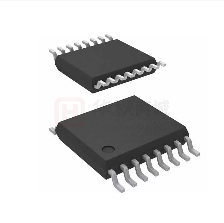
PACKAGES: SOIC-16(SOP16), SSOP-16,
TSSOP-16 and QFN-3×3-16L
DESCRIPTION
The RS2253 is a CMOS analog IC configured as
three single-pole/double-throw (SPDT) switches. This
CMOS device can operate from 2.5 V to 5.5 V.
The RS2253 device are digitally-controlled analog
switches. It has low on-resistance (48Ω TYP) and
very low off-leakage current (1nA TYP).
The RS2253 is available in Green SOIC-16, SSOP16, TSSOP-16 and QFN-3×3-16L packages. It
operates over an ambient temperature range of -40°C
to +125°C.
Functional Diagrams of RS2253
APPLICATIONS
•
Sensors
•
•
Analog and Digital Multiplexing and
Demultiplexing
A/D and D/A Conversion
•
Signal Gating
•
Battery-Operated Equipment
•
•
Factory Automation
Appliances
•
Communications Circuits
EN AB LE
X
Y
Z
R S2 25 3
RevC.1
1
A
X0
A
X1
B
Y0
B
Y1
C
Z0
C
Z1
www.run-ic.com
�RS2253
PIN CONFIGURATIONS
(TOP VIEW)
(TOP VIEW)
1
16
VCC
Y0
2
15
Y
Z1
3
Z
4
Z0
5
ENABLE
6
NC
7
GND
RS2253
Y1
8
14
X
13
X1
12
X0
11
A
10
B
9
Z1
Y0
Y1
VCC
16
15
14
Y
13
X
1
12
X
11
X1
10
X0
9
A
X7
Z
2
Z0
3
ENABLE
4
RS2253
EP
C
SOIC-16(SOP16)/SSOP-16/
TSSOP-16
5
6
7
8
NC
GND
C
B
QFN-3×3-16L
PIN DESCRIPTION
Y1
Y0
Z1
Z
Z0
PIN
SOIC-16/SSOP-16/
TSSOP-16
1
2
3
4
5
ENABLE
6
4
NC
GND
C
B
A
X0
X1
X
Y
7
8
9
10
11
12
13
14
15
5
6
7
8
9
10
11
12
13
VCC
16
14
EP
—
Exposed Pad
NAME
PIN
QFN-3×3-16L
FUNCTION
15
16
1
2
3
2
Analog Switch “Y” Normally Open Input.
Analog Switch “Y” Normally Closed Input.
Analog Switch “Z” Normally Open Input.
Analog Switch “Z” Output.
Analog Switch “Z” Normally Closed Input.
Digital Enable Input. Normally connected
to GND.
No Connect.
Ground. Connect to digital ground.
Digital Address “C” Input.
Digital Address “B” Input.
Digital Address “A” Input.
Analog Switch “X” Normally Closed Input.
Analog Switch “X” Normally Open Input.
Analog Switch “X” Output.
Analog Switch “Y” Output.
Positive Analog and Digital Supply Voltage
Input
Exposed Pad. Connect EP to GND.
www.run-ic.com
�RS2253
FUNCTION TABLE
ENABLE
INPUT
1
0
0
0
0
0
0
0
0
INPUT STATES
C
B
X
X
0
0
0
0
0
1
0
1
1
0
1
0
1
1
1
1
A
X
0
1
0
1
0
1
0
1
ON CHANNEL(S)
NONE
X0, Y0, Z0
X1, Y0, Z0
X0, Y1, Z0
X1, Y1, Z0
X0, Y0, Z1
X1, Y0, Z1
X0, Y1, Z1
X1, Y1, Z1
X=Don’t care
NOTE: Input and output pins are identical and inter-changeable. Either may be considered an input or
output; signals pass equally well in either direction.
3
www.run-ic.com
�RS2253
ABSOLUTE MAXIMUM RATINGS (1)
VCC to GND..........................................................−0.3 to 6V
Input Terminals, Voltage. (2) .................– 0.3 to (V+) + 0.3V
Continuous Current into Any Terminal......................±20mA
Peak Current, X_
(Pulsed at 1ms,10% duty cycle)…………………….. ±40mA
Storage Temperature ……….…………… −65°C to +150°C
Operating Temperature ……….…….…… −40°C to +125°C
Junction Temperature...............................................+150°C
Package Thermal Resistance @ TA = +25°C
ESD SENSITIVITY CAUTION
ESD damage can range from subtle performance
degradation to complete device failure. Precision
integrated circuits may be more susceptible to
damage because very small parametric changes
could cause the device not to meet its published
specifications.
QFN-3×3-16L………………….………..……………. 80°C/W
SSOP-16……….…………........................................64°C/W
SOIC-16, TSSOP-16………….……….…………….100°C/W
Lead Temperature (Soldering, 10s) …………….........260°C
ESD Susceptibility
HBM ….......................................................................1000V
MM ……………………….........………………...……….100V
(1) Stresses above these ratings may cause permanent damage. Exposure
to absolute maximum conditions for extended periods may degrade
device reliability. These are stress ratings only, and functional
operation of the device at these or any other conditions beyond those
specified is not implied.
(2) Input terminals are diode-clamped to the power-supply rails. Input
signals that can swing more than 0.3V beyond the supply rails should
be current-limited to 10mA or less.
PACKAGE/ORDERING INFORMATION
PRODUCT
TEMPERATURE
RANGE
PACKAGE LEAD
PACKAGE
MARKING
RS2253XS16
-40°C ~+125°C
SOIC-16(SOP16)
RS2253
Tape and Reel,3000
RS2253XSS16
-40°C ~+125°C
SSOP-16
RS2253
Tape and Reel,3000
RS2253XTSS16
-40°C ~+125°C
TSSOP-16
RS2253
Tape and Reel,3000
RS2253XTQC16
-40°C ~+125°C
QFN-3×3 -16L
RS2253
Tape and Reel,3000
ORDERING NUMBER
PACKAGE OPTION
RS2253
4
www.run-ic.com
�RS2253
ELECTRICAL CHARACTERISTICS
VCC = 5.0 V or 3.3V, FULL= –40°C to +125°C, Typical values are at TA = +25°C. (unless otherwise noted)
PARAMETER
SYMBOL
CONDITIONS
VCC
TA
MIN
TYP
MAX UNITS
ANALOG SWITCH
Analog Signal Range
VX_, VY_, VZ_
VX, VY, VZ
FULL
VCC=5V, IX, IY, IZ =1mA
On-Resistance
RON
VCC=3.3V, IX, IY, IZ =1mA
On-Resistance Match
Between Channels
On-Resistance Flatness
X_, Y_, Z_ Off
Leakage Current
X, Y, Z Off
Leakage Current
X, Y, Z On
Leakage Current
5V
3.3V
∆RON
VCC=5V, IX, IY, IZ =1mA
5V
RFLAT(ON)
VCC=5V, IX, IY, IZ =1mA
5V
VX_, VY_, VZ_=1V, 4.5V
IX_(OFF) IY_(OFF) VX, VY, VZ =4.5V, 1V
IZ_(OFF)
VX_, VY_, VZ_=1V, 3V
VX, VY, VZ =3V, 1V
VX_, VY_, VZ_=1V, 4.5V
IX(OFF) IY(OFF) VX, VY, VZ =4.5V, 1V
IZ(OFF)
VX_, VY_, VZ_=1V, 3V
VX, VY, VZ =3V, 1V
GND
+25°C
48
FULL
+25°C
100
FULL
+25°C
1.5
FULL
+25°C
17
FULL
VCC
V
65
Ω
70
Ω
130
Ω
140
Ω
5
Ω
5.3
Ω
25
Ω
28
Ω
5V
+25°C
1
100
nA
3.3V
+25°C
1
100
nA
5V
+25°C
1
100
nA
3.3V
+25°C
1
100
nA
VCC=5V, VX, VY, VZ =4.5V, 1V
5V
+25°C
1
100
nA
VCC=3.3V, VX, VY, VZ =3V, 1V
3.3V
+25°C
1
100
nA
5V
+25°C
1.7
V
3.3V
+25°C
1.7
V
5V
+25°C
0.5
V
3.3V
+25°C
0.5
V
IX(ON) IY(ON) IZ(ON)
DIGITAL CONTROL INPUTS(1)
Logic Input Logic
Threshold High
VAH, VBH, VCH,
V̅̅̅̅̅̅̅̅̅̅̅̅
ENABLE
Logic Input Logic
Threshold Low
VAL, VBL, VCL
V̅̅̅̅̅̅̅̅̅̅̅̅
ENABLE
Input-Current High
IAH, IBH, ICH
I̅̅̅̅̅̅̅̅̅̅̅̅
ENABLE
VA, VB, VC, V̅̅̅̅̅̅̅̅̅̅̅̅
ENABLE = VCC
3.3V to 5V +25°C
1
100
nA
Input-Current Low
IAL, IBL, ICL
I̅̅̅̅̅̅̅̅̅̅̅̅
ENABLE
VA, VB, VC, V̅̅̅̅̅̅̅̅̅̅̅̅
ENABLE = 0V
3.3V to 5V +25°C
1
100
nA
(1) All unused digital inputs of the device must be held at VIO or GND to ensure proper device operation.
5
www.run-ic.com
�RS2253
ELECTRICAL CHARACTERISTICS (continued)
VCC= 5.0 V or 3.3V, FULL= –40°C to +125°C Typical values are at TA = +25°C (unless otherwise noted)
PARAMETER
SYMBOL
CONDITIONS
tTRANS
VX_, VY_, VZ_= 3V/0V, RL = 300Ω,
CL = 35pF, Test Circuit 1
VX_, VY_, VZ_= 3V/0V, RL = 300Ω,
CL = 35pF, Test Circuit 1
VCC
TEMP
MIN
TYP
MAX UNITS
5V
+25°C
160
ns
3.3V
+25°C
240
ns
DYNAMIC CHARACTERISTICS
Address Transition Time
ENABLE Turn-On Time
tON
VX_, VY_, VZ_= 3V, RL = 300Ω,
CL = 35pF, Test Circuit 2
ENABLE Turn-Off Time
tOFF
VX_, VY_, VZ_= 3V, RL = 300Ω,
CL = 35pF, Test Circuit 2
Internal A, B, C Rise Time
tR
Internal A, B, C Fall Time
tF
Break-Before-Make Time Delay
tD
Charge Injection
Q
5V
3.3V
5V
3.3V
5V
3.3V
5V
3.3V
VX_, VY_, VZ_= 3V, RL = 300Ω,
CL = 35pF, Test Circuit 3
5V
3.3V
RS = 0Ω, CL = 1nF, Test Circuit 4
5V
RS = 0Ω, CL = 1nF, Test Circuit 4
3.3V
90
140
70
100
+25°C
+25°C
ns
ns
50
+25°C
ns
80
+25°C
+25°C
+25°C
60
85
ns
ns
60
ns
90
ns
6
pC
4
pC
Off Isolation
OISO
RL = 50Ω, f = 1MHz, Test Circuit 5
5V
+25°C
-83
dB
Channel-to-Channel Crosstalk
XTALK
RL = 50Ω, f = 1MHz, Test Circuit 5
5V
+25°C
-110
dB
180
MHz
180
MHz
-3dB Bandwidth
Input Off-Capacitance
Output Off-Capacitance
Output On- Capacitance
Total Harmonic Distortion
BW
CX_(OFF)
CY_(OFF)
CZ_(OFF)
CX(OFF) CY(OFF)
CZ(OFF)
CX(ON) CY(ON)
CZ(ON)
THD
5V
RL = 50Ω
3.3V
VX_, VY_, VZ_= 0V, f = 1MHz,
Test Circuit 6
VX_, VY_, VZ_= 0V, f = 1MHz,
Test Circuit 6
VX_, VY_, VZ_= 0V, f = 1MHz,
Test Circuit 6
RL = 600Ω,5VP-P, f = 20Hz to
20kHz
+25°C
5V
+25°C
4.7
pF
5V
+25°C
12.7
pF
5V
+25°C
16
pF
5V
+25°C
0.7
%
POWER REQUIREMENTS
Power Supply Range
Power Supply Current
VCC
ICC
FULL
VCC = 5.0V, VA, VB, VC,
V̅̅̅̅̅̅̅̅̅̅̅̅
ENABLE = VCC or 0
VCC = 3.3V, VA, VB, VC,
V̅̅̅̅̅̅̅̅̅̅̅̅
ENABLE = VCC or 0
6
2.5
5.5
V
5V
+25°C
0.001
2
μA
3.3V
+25°C
0.001
1
μA
www.run-ic.com
�RS2253
TYPICAL CHARACTERISTICS
Typical ron as a Function of Input Voltage (VI ) for VI = 0 to V+
400
Ron(Ω)
200
100
50
25
0
0.5
1
1.5
2
2.5
3
3.5
4
4.5
5
5.5
VI(V)
V+=5.5V
V+=4.5V
V+=3.3V
7
V+=2.5V
www.run-ic.com
�RS2253
Parameter Measurement Information
Test Circuit 1. Address Transition Times (tTRANS)
Test Circuit 2. Switching Times (tON, tOFF)
Test Circuit 3. Break-Before-Make Time Delay (tD)
8
www.run-ic.com
�RS2253
Parameter Measurement Information (continued)
Test Circuit 4. Charge Injection (Q)
Test Circuit 5. Off Isolation, On Loss
Test Circuit 6. Capacitance
9
www.run-ic.com
�RS2253
APPLICATION NOTES
The RS2253 device is a triple 2-channel multiplexer having three separate digital control inputs, A, B, and C,
and an inhibit input. Each control input selects one of a pair of channels which are connected in a single-pole,
double-throw configuration.
When the devices are used as demultiplexers, the CHANNEL IN/OUT terminals are the outputs and the
COMMON OUT/IN terminals are the inputs.
LOGIC
LEVEL
CONVERSION
16 VCC
BINARY TO
1 OF 2
DECODERS
WITH
INHIBIT
IN/OUT
Z1
Z0
Y1
Y0
X1
X0
3
5
1
2
13
12
TG
COMMON
OUT/IN
X
14
A 11
TG
TG
COMMON
OUT/IN
Y
15
B 10
C
TG
TG
9
COMMON
OUT/IN
Z
4
TG
ENABLE 6
VCC
8
GND
7
NC
Figure 1. The RS2253 Functional Block Diagram
10
www.run-ic.com
�RS2253
PACKAGE OUTLINE DIMENSIONS
SOIC-16
e
b
5.2
1.27
E1 E
0.6
D
1.27
RECOMMENDED LAND PATTERN (Unit: mm)
A2
A1
A
c
θ
L
Symbol
Dimensions In Millimeters
Dimensions In Inches
Min
Max
Min
Max
A
1.350
1.750
0.053
0.069
A1
0.100
0.250
0.004
0.010
A2
1.350
1.550
0.053
0.061
b
0.330
0.510
0.013
0.020
c
0.170
0.250
0.006
0.010
D
9.800
10.200
0.386
0.402
E
3.800
4.000
0.150
0.157
E1
5.800
6.200
0.228
0.244
e
1.27(BSC)
0.050(BSC)
L
0.400
1.270
0.016
0.050
θ
0°
8°
0°
8°
11
www.run-ic.com
�RS2253
SSOP-16
e
b
5.588
E1 E
1.651
D
0.635
0.406
RECOMMENDED LAND PATTERN (Unit: mm)
A2
A1
Symbol
H
C
A
θ
L
Dimensions In Millimeters
Dimensions In Inches
Min
Max
Min
Max
A
1.350
1.750
0.053
0.069
A1
0.100
0.250
0.004
0.010
A2
1.350
1.550
0.053
0.061
b
0.200
0.300
0.008
0.012
c
0.170
0.250
0.007
0.010
D
4.700
5.100
0.185
0.200
E
3.800
4.000
0.150
0.157
E1
5.800
6.200
0.228
0.244
e
0.635(BSC)
0.025(BSC)
L
0.400
1.270
0.016
0.050
θ
0°
8°
0°
8°
12
www.run-ic.com
�RS2253
TSSOP-16
e
b
5.94
E1 E
1.78
D
0.65
0.42
RECOMMENDED LAND PATTERN (Unit: mm)
A2
A1
Symbol
H
C
A
θ
L
Dimensions In Millimeters
Min
Max
A
Dimensions In Inches
Min
Max
1.200
0.047
A1
0.050
0.150
0.002
0.006
A2
0.800
1.050
0.031
0.041
b
0.190
0.300
0.007
0.012
c
0.090
0.200
0.004
0.008
D
4.860
5.100
0.191
0.201
E
4.300
4.500
0.169
0.177
E1
6.200
6.600
0.244
0.260
e
L
0.650(BSC)
0.500
H
θ
0.026(BSC)
0.700
0.02
0.25TYP
1°
0.028
0.01TYP
7°
13
1°
7°
www.run-ic.com
�RS2253
QFN-3x3-16L
E
e
L
b
E1
D
D1
N16
N5
N1
TOP VIEW
BOTTOM VIEW
0.50
1.70
A1
A2
3.60
A
0.70
0.24
SIDE VIEW
1.70
RECOMMENDED LAND PATTERN
(Unit: mm)
Symbol
Dimensions In Millimeters
Dimensions In Inches
Min
Max
Min
Max
A
0.700
0.800
0.028
0.031
A1
0.000
0.050
0.000
0.002
A2
0.203
0.008
b
0.180
0.300
0.007
0.012
D
2.900
3.100
0.114
0.122
D1
1.600
1.800
0.063
0.071
E
2.900
3.100
0.114
0.122
E1
1.600
1.800
0.063
0.071
e
L
0.500 TYP
0.300
0.020 TYP
0.500
14
0.012
0.020
www.run-ic.com
�