MYD-Y6ULG2-256N256D-50-I 数据手册
MYD-Y6ULX Development Board
MYC-Y6ULX CPU Module as Controller Board
528Hz NXP i.MX 6UL/6ULL ARM Cortex-A7 Processors
1.0mm pitch 140-pin Stamp Hole Expansion Interface for Board-to-Board Connections
256MB DDR3 SDRAM, 256MB Nand Flash or 4GB eMMC Flash
2 x USB2.0 Host, 1 x USB2.0 OTG, 2 x 10/100 Mbps Ethernets , CAN, RS485, TF, LCD, Camera, Audio…
Onboard SDIO based WiFi Module with External Antennas
Mini-PCIe Slot for Optional USB based 4G LTE Module
Optional 4.3 or 7 inch LCD/TSP and Camera Module
Ready-to-Run Linux 4.1.15
Figure 1-1 MYD-Y6ULX Development Board
Description
The MYD-Y6ULX development board is a complete evaluation platform for NXP’s i.MX 6UltraLite / 6ULL processor
family, which can operate at 528 MHz and features the most efficient ARM Cortex-A7 core, providing various
memory interfaces and enhancing the flexibility and convenience of the board to connect peripheral devices. The
board is ready to run Linux and supports industrial operating temperature range from -40 to +85 Celsius.
The MYD-Y6ULX development board employs the MYC-Y6ULX CPU Module as the controller board by populating
the CPU Module on its base board through 1.0mm pitch 140-pin stamp hole interface. The MYC-Y6ULX
1 / 11
�CPU Module is mounted with a shield cover and integrated with core components including i.MX 6UltraLite /
6ULL processor, 256MB DDR3, 256MB Nand Flash or optional 4GB eMMC and Ethernet PHY. The base board has
extended rich peripherals through connectors and headers like Serial ports, USB, Ethernet, CAN, Micro SD card,
WiFi module, LCD/Touch screen, Camera, Audio as well as an optional Mini PCIe interface for USB based 4G LTE
module. It is a versatile platform and solid reference design delivered with necessary cable accessories detailed
documentations ideal for prototype and evaluation based on i.MX 6UL/6ULL solutions.
MYIR offers three models of MYD-Y6ULX development boards with mainly different features as shown in below
table. User can select model according to their own requirement.
MYD-Y6ULX
MYD-Y6ULG2-256N256D-50-I
MYD-Y6ULY2-256N256D-50-C
MYD-Y6ULY2-4E512D-50-C
Processor
MCIMX6G2CVM05AB
MCIMX6Y2DVM05AA
MCIMX6Y2DVM05AA
MYC-Y6ULX
RAM
Flash
WiFi
Working
Temp.
MYC-Y6ULG2-256N256D-50-I
256MB DDR3
256MB Nand Flash
Support
-40 to +85 Celsius
MYC-Y6ULY2-256N256D-50-C
256MB DDR3
256MB Nand Flash
Support
0 to +70 Celsius
WiFi Module can only support -20 to +65 Celsius.
MYC-Y6ULY2-4E512D-50-C
512MB DDR3
4GB eMMC
Cannot support
Reuse SDIO with eMMC
0 to +70 Celsius
Table 1-1 Three Models of MYD-6ULX (default configurations)
2 / 11
�Hardware Specification
The MYC-Y6ULX CPU Module is using the 14 x 14mm, 0.8 mm ball pitch, 289 MAPBGA package 528 MHz i.MX
6UltraLite / i.MX 6ULL ARM Cortex-A7 application processor which provides multiple compatible options of G0,
G1, G2, G3, Y0, Y1 and Y2 sub family. The MCIMX6G2CVM05AB and MCIMX6Y2DVM05AA are optional as the
default part with the board.
Expanding the i.MX 6 series, the i.MX 6UltraLite is a high performance, ultra-efficient processor family featuring
an advanced implementation of a single ARM® Cortex®-A7 core, which operates at speeds up to 696 MHz. The
i.MX 6UltraLite applications processor includes an integrated power management module that reduces the
complexity of external power supply and simplifies power sequencing. Each processor in this family provides
various memory interfaces, including 16-bit LPDDR2, DDR3, DDR3L, raw and managed NAND flash, NOR flash,
eMMC, Quad SPI and a wide range of other interfaces for connecting peripherals such as WLAN, Bluetooth™, GPS,
displays and camera sensors.
Feature
MCIMX6G0
MCIMX6G1
MCIMX6G2
MCIMX6G3
Speed
528 MHz
528 MHz, 696 MHz
528 MHz, 696 MHz
528 MHz
128 KB L2
128 KB L2
Cache
OCRAM
DRAM
eFuse
NAND (BCH40)
EBI
Ethernet
USB
CAN
Security
Graphic
CSI
LCD
Quad SPI
SDIO
UART
I2C
SPI
I2S/SAI
S/PDIF
Timer/PWM
12-bit ADC
3 / 11
32 KB-I, 32 KB-D
128 KB
32 KB-I, 32 KB-D
128 KB
32 KB-I, 32 KB-D
32 KB-I, 32 KB-D
128 KB
128 KB
128 KB L2
16-bit LP-DDR2,
16-bit LP-DDR2,
16-bit LP-DDR2,
16-bit LP-DDR2,
512-bit
1024-bit
1536-bit
2048-bit
DDR3/DDR3L
Yes
DDR3/DDR4L
Yes
Yes
Yes
DDR3/DDR5L
Yes
Yes
DDR3/DDR6L
Yes
Yes
10/100-Mbit/s x 1
10/100-Mbit/s x 1
10/100-Mbit/s x 2
10/100-Mbit/s x 2
0
1
2
2
OTG, HS/FS x 1
Basic
OTG, HS/FS x 2
OTG, HS/FS x 2
TRNG, Crypto Engine
TRNG, Crypto Engine
Secure Boot
Secure Boot
(AES/TDES/SHA),
(AES/TDES/SHA),
TRNG, Crypto Engine (AES
with DPA/TDES/SHA/RSA),
Secure Boot, tamper monitor,
PCI4.0 pre-certification,
OTF DRAM encryption
None
None
None
None
24-bit Parallel LCD
24-bit Parallel LCD
2
2
2
None
None
1
1
2
4
8
2
4
2
4
1
1
3
Timer x 2, PWM x 4
1 x 10-ch.
1
Timer x 4, PWM x 8
1 x 10-ch.
PxP
OTG, HS/FS x 2
24-bit Parallel CSI
1
8
4
4
3
1
Timer x 4, PWM x 8
2 x 10-ch.
Table 1-2 i.MX 6UltraLite Device Options
PxP
24-bit Parallel CSI
1
8
4
4
3
1
Timer x 4, PWM x 8
2 x 10-ch.
�The i.MX 6ULL is a power efficient and cost optimized applications processor family featuring an advanced
implementation of a single ARM Cortex-A7 core, which operates at speeds up to 900 MHz. The i.MX 6ULL
applications processor includes an integrated power management module that reduces the complexity of an
external power supply and simplifies power sequencing. Each processor in this family provides various memory
interfaces, including 16-bit LPDDR2, DDR3, DDR3L, raw and managed NAND flash, NOR flash, eMMC, Quad SPI
and a wide range of other interfaces for connecting peripherals such as WLAN, Bluetooth®, GPS, displays and
camera sensors.
Feature
MCIMX6Y0
MCIMX6Y1
MCIMX6Y2
Core
ARM® Cortex-A7
ARM® Cortex-A7
ARM® Cortex-A7
32 KB-I, 32 KB-D
32 KB-I, 32 KB-D
128 KB
128 KB
Speed
Cache
OCRAM
DRAM
eFuse
NAND (BCH40)
EBI
Ethernet
USB
CAN
Graphic
CSI
LCD
Quad SPI
SDIO
UART
I2C
SPI
I2S/SAI
ESAI
S/PDIF
Timer/PWM
12-bit ADC
Security
Temperature
528 MHz
32 KB-I, 32 KB-D
128 KB
528 MHz
128 KB L2
128 KB L2
16-bit LP-DDR2,
16-bit LP-DDR2,
16-bit LP-DDR2,
256-bit
256-bit
256-bit
DDR3/DDR3L
Yes
Yes
DDR3/DDR4L
Yes
Yes
DDR3/DDR5L
Yes
Yes
10/100-Mbit/s x 1
10/100-Mbit/s x 1
10/100-Mbit/s x 2
0
1
2
OTG, HS/FS x 1
OTG, HS/FS x 2
OTG, HS/FS x 2
None
None
None
None
24-bit Parallel LCD
2
2
None
1
2
4
2
2
1
1
1
None
1
8
4
4
3
1
1
PxP
16-bit Parallel CSI
1
8
4
4
3
1
1
Timer x 2, PWM x 4
Timer x 4, PWM x 8
Timer x 4, PWM x 8
None
AES-128, HAB
AES-128, HAB
1 x 10-ch.
-40°C to 105°C (Tj)
1 x 10-ch.
-40°C to 105°C (Tj)
Table 1-3 i.MX 6ULL Device Options
4 / 11
528 MHz
2 x 10-ch.
0°C to 90°C (Tj)
�Mechanical Parameters
• Dimensions: 105mm x 140mm (base board), 37mm x 39mm (CPU Module)
• PCB Layers: 4-layer design (base board), 8-layer design (CPU Module)
• Power supply: +12V/1.5A (base board), +3.3V/0.3A (CPU Module)
• Working temperature: 0~70 Celsius (commercial grade) or -40~85 Celsius (industrial grade)
The MYD-Y6ULX Controller Board (MYC-Y6ULX CPU Module)
Figure 1-2 MYC-Y6ULX CPU Module (delivered with shield cover)
Processor
•
528MHz NXP i.MX 6UltraLite / i.MX 6ULL ARM Cortex-A7 processor
(MCIMX6G2CVM05AB or MCIMX6Y2DVM05AA by default)
Memory
•
•
256MB DDR3 SDRAM (supports up to 1GB)
256MB Nand Flash (4GB eMMC Flash is optional)
Peripherals and Signals Routed to Pins
MYC-Y6ULX Pinouts Description
• One 10/100M Ethernet PHY
• 1.0mm pitch 140-pin stamp hole expansion interface
- 2 x 10/100Mbps Ethernet
- 8 x Serial ports
- 4 x I2C
- 2 x CAN
- 4 x SPI
- 8 x ADC
- 8 x PWM
- 3 x I2S
- 1 x Parallel Camera Sensor Interface
5 / 11
�- 1 x JTAG
- 1 x 24-bit LCD interface
- Up to 97 x GPIOs
Note: the peripheral signals brought out to the expansion interface are listed in maximum number. Some signals
are reused. Please refer to the processor datasheet.
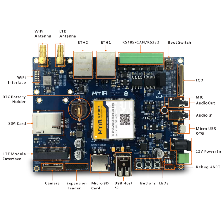
The MYD-Y6ULX Base Board
Figure 1-3 MYD-Y6ULX Base Board
•
•
•
•
•
•
•
•
•
•
•
•
•
•
6 / 11
Serial ports
- 1 x Debug serial port (TTL)
- 1 x RS485 serial port (with isolation)
- 1 x 3-wire RS232 serial port (with isolation)
USB
- 2 x USB2.0 Host ports
- 1 x Micro USB2.0 OTG ports
1 x Mini PCIe interface (for optional USB based 4G LTE module)
1 x SIM card socket
1 x SDIO based WiFi module
2 x External antenna interfaces (one for WiFi module and one for 4G LTE module)
2 x 10/100 Mbps Ethernet interfaces
1 x Camera interface
1 x CAN interface (with isolation)
1 x Micro SD card slot
1 x LCD interface (16-bit true color, supports optional 4.3-inch and 7-inch TFT LCD)
Battery backed RTC
Audio input/output port (3.5mm jack)
3 x Buttons (1 x Reset button, 1 x User button, 1 x ON/OFF button)
�•
•
2 x LEDs (1 x power indicator LED, 1 x user-defined LED)
1 x 2.0mm 20-pin male expansion connector
- 1 x SPI
- 1 x I2C
- 2 x UART
- 10 x GPIO
Figure 1-4 MYD-Y6ULX Development Board
7 / 11
�Function Block Diagram
Figure 1-5 MYC-Y6ULX Function Block Diagram
Figure 1-6 MYD-Y6ULX Function Block Diagram
8 / 11
�Dimension Chart of MYD-Y6ULX
Figure 1-7 Dimension Chart of MYD-Y6ULX
9 / 11
�Software Features
The MYD-Y6ULX development board supports running Linux Operating System and is provided with software
packages. Software features are summarized as below:
Item
Bootstrap program
Kernel
Features
Description
u-boot
The primary bootstrap (source code)
USB
HOST and OTG driver (source code)
Version
Linux 4.1.15 (source code, based on official imx_4.1.15_2.0.0_ga
version)
Ethernet
Ethernet driver (source code)
MMC
MMC/eMMC/TF card driver (source code)
NandFlash
Nand Flash driver (source code)
eMMC
eMMC driver (source code)
WiFi
WiFi Module driver (SDIO signal, source code)
4G LTE
Camera
Linux Drivers
LCD Controller
Touch Panel
RTC
GPIO Button
GPIO LED
GPIO KEY
UART
LCD driver (source code, supports MYIR’s 4.3- and 7- inch LCD)
Resistive and Capacitive touch screen driver (source code)
RTC driver (source code)
Button driver (source code)
LED driver (source code)
KEY driver (source code)
CAN driver (source code)
RS485
RS485 driver (source code)
Audio
Audio (wm8904) driver (source code)
UART
Compiler Tool Chain
Camera driver (source code, supports MYIR’s MY-CAM011B)
UART driver (source code)
CAN
File System
4G LTE Module driver (USB signal, source code)
UART driver (source code)
SPI
SPI driver (source code)
I2C
Yocto
Linaro GCC 4.9 hf
MetaToolchain
Applications
Tool Chain
I2C driver (source code)
Including QT5.6 (source code)
Binary file
Built by Yocto, GCC 5.3 (Binary file)
Built by Yocto, GCC 5.3 (Binary file)
Table 1-4 Software Features of MYD-Y6ULX
10 / 11
�Order Information
Product Item
MYD-Y6ULX Development Board
MYC-Y6ULX CPU Module
MY-LCD43TP 4.3-inch LCD Module
with resistive touch screen
MY-LCD70TP 7-inch LCD Module
with resistive touch screen
MY-LCD70TP-C 7-inch LCD Module
with capacitive touch screen
MY-CAM011B Camera Module
Part No.
Packing List
MYD-Y6ULG2-256N256D-50-I
One MYD-Y6ULX Development Board
One 12V/1.5A Power adapter
One USB cable
One Ethernet cable
One 4G LTE antenna
One WiFi antenna
(MYC-Y6ULY2-4E512D-50-C has none.)
One Product Disk
(including user manual, datasheet, base
board schematic, CPU module pinouts
and software packages)
MYD-Y6ULY2-256N256D-50-C
MYD-Y6ULY2-4E512D-50-C
MYC-Y6ULG2-256N256D-50-I
MYC-Y6ULY2-256N256D-50-C
MYC-Y6ULY2-4E512D-50-C
MY-TFT043RV2
MY-TFT070RV2
MY-TFT070CV2
MY-CAM011B
MYIR Tech Limited
Room 04, 6th Floor, Building No.2, Fada Road, Yunli Intelligent Park,
Bantian, Longgang District, Shenzhen, Guangdong, China 518129
E-mail: sales@myirtech.com
Phone: +86-755-22984836
Fax: +86-755-25532724
Website: http://www.myirtech.com
11 / 11
Add-on Options
MYC-Y6ULX CPU Module
MY-LCD43TP 4.3-inch LCD Module
MY-LCD70TP 7-inch LCD Module
MY-LCD70TP-C 7-inch LCD Module
MY-CAM011B Camera Module
�