PH2925U,115

PH2925U,115

  • 厂商:

    NEXPERIA(安世)

  • 封装:

    SOT669

  • 描述:

    MOS管 N-Channel VDS=25V VGS=±10V ID=100mA RDS(ON)=3mΩ@4.5V SOT669

  • 详情介绍
  • 数据手册
  • 价格&库存
PH2925U,115 数据手册
PH2925U N-channel TrenchMOS ultra low level FET Rev. 04 — 24 February 2009 Product data sheet 1. Product profile 1.1 General description Ultra low level N-channel enhancement mode Field-Effect Transistor (FET) in a plastic package using TrenchMOS technology. This product is designed and qualified for use in computing, communications, consumer and industrial applications only. 1.2 Features and benefits „ Higher operating power due to low thermal resistance „ Low conduction losses due to low on-state resistance „ Interfaces directly with low voltage gate drivers 1.3 Applications „ DC-to-DC convertors „ Portable equipment „ Notebook computers „ Switched-mode power supplies 1.4 Quick reference data Table 1. Quick reference Symbol Parameter Conditions Min Typ Max Unit VDS drain-source voltage Tj ≥ 25 °C; Tj ≤ 150 °C - - 25 V ID drain current Tmb = 25 °C; VGS = 4.5 V; see Figure 1; see Figure 3 - - 100 A Ptot total power dissipation Tmb = 25 °C; see Figure 2 - - 62.5 W VGS = 4.5 V; ID = 50 A; VDS = 10 V; Tj = 25 °C; see Figure 10; see Figure 11 - 20.2 - nC VGS = 4.5 V; ID = 25 A; Tj = 25 °C; see Figure 8; see Figure 9 - 2.3 3 mΩ Dynamic characteristics QGD gate-drain charge Static characteristics RDSon drain-source on-state resistance PH2925U Nexperia N-channel TrenchMOS ultra low level FET 2. Pinning information Table 2. Pinning information Pin Symbol Description Simplified outline 1 S source 2 S source 3 S source 4 G gate mb D mounting base; connected to drain Graphic symbol mb D G S mbb076 1 2 3 4 SOT669 (LFPAK) 3. Ordering information Table 3. Ordering information Type number Package Name Description PH2925U LFPAK plastic single-ended surface-mounted package (LFPAK); 4 leads Version SOT669 4. Limiting values Table 4. Limiting values In accordance with the Absolute Maximum Rating System (IEC 60134). Symbol Parameter Conditions Min Max Unit VDS drain-source voltage Tj ≥ 25 °C; Tj ≤ 150 °C - 25 V VDGR drain-gate voltage Tj ≤ 150 °C; Tj ≥ 25 °C; RGS = 20 kΩ - 25 V VGS gate-source voltage -10 10 V ID drain current VGS = 4.5 V; Tmb = 100 °C; see Figure 1 - 70 A VGS = 4.5 V; Tmb = 25 °C; see Figure 1; see Figure 3 - 100 A - 300 A IDM peak drain current tp ≤ 10 µs; pulsed; Tmb = 25 °C; see Figure 3 Ptot total power dissipation Tmb = 25 °C; see Figure 2 - 62.5 W Tstg storage temperature -55 150 °C Tj junction temperature -55 150 °C Source-drain diode IS source current Tmb = 25 °C - 52 A ISM peak source current tp ≤ 10 µs; pulsed; Tmb = 25 °C - 150 A - 250 mJ Avalanche ruggedness EDS(AL)S non-repetitive VGS = 10 V; Tj(init) = 25 °C; ID = 70.7 A; Vsup ≤ 25 V; drain-source avalanche unclamped; tp = 0.22 ms; RGS = 50 Ω energy PH2925U_4 Product data sheet Rev. 04 — 24 February 2009 2 of 12 © Nexperia B.V. 2017. All rights reserved PH2925U Nexperia N-channel TrenchMOS ultra low level FET 003aaa631 120 03aa15 120 Ider (%) Pder (%) 80 80 40 40 0 0 0 Fig 1. 50 100 150 Tmb (°C) 200 Normalized continuous drain current as a function of mounting base temperature 0 50 100 150 200 Tmb (°C) Fig 2. Normalized total power dissipation as a function of mounting base temperature 003aaa438 103 ID (A) Limit RDSon = VDS/ ID tp = 10 μ s 102 100 μ s 1 ms 10 ms 10 DC 100 ms 1 10-1 10-1 Fig 3. 1 10 102 VDS (V) Safe operating area; continuous and peak drain currents as a function of drain-source voltage PH2925U_4 Product data sheet Rev. 04 — 24 February 2009 3 of 12 © Nexperia B.V. 2017. All rights reserved PH2925U Nexperia N-channel TrenchMOS ultra low level FET 5. Thermal characteristics Table 5. Thermal characteristics Symbol Parameter Conditions Rth(j-mb) thermal resistance from see Figure 4 junction to mounting base Min Typ Max Unit - - 2 K/W 003aaa439 10 Zth(j-mb) (K/W) 1 δ = 0.5 δ= P 0.2 tp T 0.1 0.05 0.02 10-1 10-4 Fig 4. t tp single pulse 10-3 T 10-2 10-1 tp (s) 1 Transient thermal impedance from junction to mounting base as a function of pulse duration PH2925U_4 Product data sheet Rev. 04 — 24 February 2009 4 of 12 © Nexperia B.V. 2017. All rights reserved PH2925U Nexperia N-channel TrenchMOS ultra low level FET 6. Characteristics Table 6. Symbol Characteristics Parameter Conditions Min Typ Max Unit Static characteristics V(BR)DSS VGS(th) IDSS IGSS RDSon RG drain-source breakdown voltage gate-source threshold voltage drain leakage current gate leakage current drain-source on-state resistance ID = 250 µA; VGS = 0 V; Tj = -55 °C 22.5 - - V ID = 250 µA; VGS = 0 V; Tj = 25 °C 25 - - V ID = 1 mA; VDS = VGS; Tj = -55 °C; see Figure 6; see Figure 7 - - 1.2 V ID = 1 mA; VDS = VGS; Tj = 150 °C; see Figure 6; see Figure 7 0.25 - - V ID = 1 mA; VDS = VGS; Tj = 25 °C; see Figure 7; see Figure 6 0.45 0.7 0.95 V VDS = 25 V; VGS = 0 V; Tj = 150 °C - - 500 µA VDS = 25 V; VGS = 0 V; Tj = 25 °C - 0.06 1 µA VGS = 10 V; VDS = 0 V; Tj = 25 °C - 20 100 nA VGS = -10 V; VDS = 0 V; Tj = 25 °C - 20 100 nA VGS = 4.5 V; ID = 25 A; Tj = 150 °C; see Figure 8; see Figure 9 - 3.6 4.8 mΩ VGS = 2.5 V; ID = 25 A; Tj = 25 °C - 3.2 4.2 mΩ VGS = 4.5 V; ID = 25 A; Tj = 25 °C; see Figure 8; see Figure 9 - 2.3 3 mΩ - 1.55 - Ω internal gate resistance f = 1 MHz; Tj = 25 °C (AC) Dynamic characteristics QG(tot) total gate charge QGS gate-source charge QGD gate-drain charge VGS(pl) gate-source plateau voltage Ciss input capacitance Coss output capacitance Crss reverse transfer capacitance td(on) turn-on delay time tr rise time td(off) tf ID = 50 A; VDS = 10 V; VGS = 4.5 V; Tj = 25 °C; see Figure 10; see Figure 11 - 92 - nC - 12 - nC - 20.2 - nC ID = 50 A; VDS = 10 V; Tj = 25 °C; see Figure 10; see Figure 11 - 1.6 - V VDS = 10 V; VGS = 0 V; f = 1 MHz; Tj = 25 °C; see Figure 12 - 6150 - pF - 1170 - pF - 814 - pF - 30 - ns - 80 - ns turn-off delay time - 258 - ns fall time - 114 - ns VDS = 10 V; RL = 1 Ω; VGS = 4.5 V; RG(ext) = 4.7 Ω; Tj = 25 °C Source-drain diode VSD source-drain voltage IS = 25 A; VGS = 0 V; Tj = 25 °C; see Figure 13 - 0.72 1.2 V trr reverse recovery time IS = 20 A; dIS/dt = -100 A/µs; VGS = 0 V; VDS = 25 V - 60 - ns PH2925U_4 Product data sheet Rev. 04 — 24 February 2009 5 of 12 © Nexperia B.V. 2017. All rights reserved PH2925U Nexperia N-channel TrenchMOS ultra low level FET 003aaa440 40 4.5 2 1.5 1.4 ID (A) 03aj64 10−3 ID (A) 1.3 30 10−4 20 1.2 min 10−5 typ max 10 1.1 VGS (V) = 1 0 0 Fig 5. 0.2 0.4 0.6 0.8 VDS (V) 1 Output characteristics: drain current as a function of drain-source voltage; typical values 10−6 0 Fig 6. 03aj65 1.2 0.6 0.8 1 VGS (V) 003aaa442 20 0.9 0.4 Sub-threshold drain current as a function of gate-source voltage 1.3 VGS (V) = 1.2 RDSon (mΩ) VGS(th) (V) 0.2 15 max typ 0.6 10 min 1.5 5 0.3 4.5 0 −60 Fig 7. 0 0 60 120 0 180 10 20 30 Tj (°C) Gate-source threshold voltage as a function of junction temperature Fig 8. ID (A) 40 Drain-source on-state resistance as a function of drain current; typical values PH2925U_4 Product data sheet Rev. 04 — 24 February 2009 6 of 12 © Nexperia B.V. 2017. All rights reserved PH2925U Nexperia N-channel TrenchMOS ultra low level FET 03af18 2 003aaa445 5 VGS (V) 4 a 1.5 3 1 2 0.5 1 0 -60 Fig 9. 0 60 120 Tj (°C) 180 Normalized drain-source on-state resistance factor as a function of junction temperature 0 0 25 50 75 QG (nC) 100 Fig 10. Gate-source voltage as a function of gate charge; typical values 003aaa443 105 VDS C (pF) ID 104 VGS(pl) Ciss VGS(th) VGS QGS1 103 QGS2 QGS Coss Crss QGD QG(tot) 003aaa508 Fig 11. Gate charge waveform definitions 102 10-1 1 10 VDS (V) 102 Fig 12. Input, output and reverse transfer capacitances as a function of drain-source voltage; typical values PH2925U_4 Product data sheet Rev. 04 — 24 February 2009 7 of 12 © Nexperia B.V. 2017. All rights reserved PH2925U Nexperia N-channel TrenchMOS ultra low level FET 003aaa444 40 IS (A) 30 20 150 °C Tj = 25 °C 10 0 0 0.2 0.4 0.6 0.8 VSD (V) 1 Fig 13. Source current as a function of source-drain voltage; typical values PH2925U_4 Product data sheet Rev. 04 — 24 February 2009 8 of 12 © Nexperia B.V. 2017. All rights reserved PH2925U Nexperia N-channel TrenchMOS ultra low level FET 7. Package outline Plastic single-ended surface-mounted package (LFPAK); 4 leads A2 A E SOT669 C c2 b2 E1 b3 L1 mounting base b4 D1 D H L2 1 2 3 e 4 w M A b 1/2 X c e A (A 3) A1 C θ L detail X y C 0 2.5 5 mm scale DIMENSIONS (mm are the original dimensions) UNIT mm A A1 A2 A3 b b2 1.20 0.15 1.10 0.50 4.41 0.25 1.01 0.00 0.95 0.35 3.62 b3 b4 2.2 2.0 0.9 0.7 c D (1) c2 D1(1) E(1) E1(1) max 0.25 0.30 4.10 4.20 0.19 0.24 3.80 5.0 4.8 3.3 3.1 e H L L1 L2 w y θ 1.27 6.2 5.8 0.85 0.40 1.3 0.8 1.3 0.8 0.25 0.1 8° 0° Note 1. Plastic or metal protrusions of 0.15 mm maximum per side are not included. OUTLINE VERSION SOT669 REFERENCES IEC JEDEC JEITA EUROPEAN PROJECTION ISSUE DATE 04-10-13 06-03-16 MO-235 Fig 14. Package outline SOT669 (LFPAK) PH2925U_4 Product data sheet Rev. 04 — 24 February 2009 9 of 12 © Nexperia B.V. 2017. All rights reserved PH2925U Nexperia N-channel TrenchMOS ultra low level FET 8. Revision history Table 7. Revision history Document ID Release date Data sheet status Change notice Supersedes PH2925U_4 20090224 Product data sheet - PH2925U_3 Modifications: • The format of this data sheet has been redesigned to comply with the new identity guidelines of NXP Semiconductors. • Legal texts have been adapted to the new company name where appropriate. PH2925U_3 20051129 Product data sheet - PH2925U-02 PH2925U-02 (9397 750 13064) 20040408 Product data - PH2925U-01 PH2925U-01 (9397 750 11407) 20030502 Product data - - PH2925U_4 Product data sheet Rev. 04 — 24 February 2009 10 of 12 © Nexperia B.V. 2017. All rights reserved PH2925U Nexperia N-channel TrenchMOS ultra low level FET 9. Legal information 9.1 Data sheet status Document status [1][2] Product status[3] Definition Objective [short] data sheet Development This document contains data from the objective specification for product development. Preliminary [short] data sheet Qualification This document contains data from the preliminary specification. Product [short] data sheet Production This document contains the product specification. [1] Please consult the most recently issued document before initiating or completing a design. [2] The term 'short data sheet' is explained in section "Definitions". [3] The product status of device(s) described in this document may have changed since this document was published and may differ in case of multiple devices. The latest product status information is available on the Internet at URL http://www.nexperia.com. 9.2 Definitions Draft — The document is a draft version only. The content is still under internal review and subject to formal approval, which may result in modifications or additions. Nexperia does not give any representations or warranties as to the accuracy or completeness of information included herein and shall have no liability for the consequences of use of such information. Short data sheet — A short data sheet is an extract from a full data sheet with the same product type number(s) and title. A short data sheet is intended for quick reference only and should not be relied upon to contain detailed and full information. For detailed and full information see the relevant full data sheet, which is available on request via the local Nexperia sales office. In case of any inconsistency or conflict with the short data sheet, the full data sheet shall prevail. 9.3 Disclaimers General — Information in this document is believed to be accurate and reliable. However, Nexperia does not give any representations or warranties, expressed or implied, as to the accuracy or completeness of such information and shall have no liability for the consequences of use of such information. Right to make changes — Nexperia reserves the right to make changes to information published in this document, including without limitation specifications and product descriptions, at any time and without notice. This document supersedes and replaces all information supplied prior to the publication hereof. Suitability for use — Nexperia products are not designed, authorized or warranted to be suitable for use in medical, military, aircraft, space or life support equipment, nor in applications where failure or malfunction of a Nexperia product can reasonably be expected to result in personal injury, death or severe property or environmental damage. Nexperia accepts no liability for inclusion and/or use of Nexperia products in such equipment or applications and therefore such inclusion and/or use is at the customer’s own risk. Applications — Applications that are described herein for any of these products are for illustrative purposes only. Nexperia makes no representation or warranty that such applications will be suitable for the specified use without further testing or modification. Quick reference data — The Quick reference data is an extract of the product data given in the Limiting values and Characteristics sections of this document, and as such is not complete, exhaustive or legally binding. Limiting values — Stress above one or more limiting values (as defined in the Absolute Maximum Ratings System of IEC 60134) may cause permanent damage to the device. Limiting values are stress ratings only and operation of the device at these or any other conditions above those given in the Characteristics sections of this document is not implied. Exposure to limiting values for extended periods may affect device reliability. Terms and conditions of sale — Nexperia products are sold subject to the general terms and conditions of commercial sale, as published at http://www.nexperia.com/profile/terms, including those pertaining to warranty, intellectual property rights infringement and limitation of liability, unless explicitly otherwise agreed to in writing by Nexperia. In case of any inconsistency or conflict between information in this document and such terms and conditions, the latter will prevail. No offer to sell or license — Nothing in this document may be interpreted or construed as an offer to sell products that is open for acceptance or the grant, conveyance or implication of any license under any copyrights, patents or other industrial or intellectual property rights. 9.4 Trademarks Notice: All referenced brands, product names, service names and trademarks are the property of their respective owners. 10. Contact information For more information, please visit: http://www.nexperia.com For sales office addresses, please send an email to: salesaddresses@nexperia.com PH2925U_4 Product data sheet Rev. 04 — 24 February 2009 11 of 12 © Nexperia B.V. 2017. All rights reserved Nexperia PH2925U N-channel TrenchMOS ultra low level FET 11. Contents 1 1.1 1.2 1.3 1.4 2 3 4 5 6 7 8 9 9.1 9.2 9.3 9.4 10 © Product profile . . . . . . . . . . . . . . . . . . . . . . . . . . .1 General description . . . . . . . . . . . . . . . . . . . . . .1 Features and benefits . . . . . . . . . . . . . . . . . . . . .1 Applications . . . . . . . . . . . . . . . . . . . . . . . . . . . .1 Quick reference data . . . . . . . . . . . . . . . . . . . . .1 Pinning information . . . . . . . . . . . . . . . . . . . . . . .2 Ordering information . . . . . . . . . . . . . . . . . . . . . .2 Limiting values. . . . . . . . . . . . . . . . . . . . . . . . . . .2 Thermal characteristics . . . . . . . . . . . . . . . . . . .4 Characteristics . . . . . . . . . . . . . . . . . . . . . . . . . . .5 Package outline . . . . . . . . . . . . . . . . . . . . . . . . . .9 Revision history . . . . . . . . . . . . . . . . . . . . . . . . .10 Legal information. . . . . . . . . . . . . . . . . . . . . . . . 11 Data sheet status . . . . . . . . . . . . . . . . . . . . . . . 11 Definitions . . . . . . . . . . . . . . . . . . . . . . . . . . . . . 11 Disclaimers . . . . . . . . . . . . . . . . . . . . . . . . . . . . 11 Trademarks. . . . . . . . . . . . . . . . . . . . . . . . . . . . 11 Contact information. . . . . . . . . . . . . . . . . . . . . . 11 Nexperia B.V. 2017. All rights reserved For more information, please visit: http://www.nexperia.com For sales office addresses, please send an email to: salesaddresses@nexperia.com Date of release: 24 February 2009
PH2925U,115
物料型号为 PH2925U,这是 Nexperia 公司生产的 N-channel TrenchMOS 超低电平 FET(场效应晶体管)。

以下是对 PDF 文档内容的中文分析:

器件简介: - PH2925U 是使用 TrenchMOS 技术的 N-channel 增强型场效应晶体管。

- 该产品适用于计算机、通信、消费电子和工业应用。

- 特点包括由于低热阻而具有更高的工作功率、由于低导通电阻而具有较低的导通损耗,以及能够直接与低电压栅极驱动器接口。


引脚分配: - 引脚 1、2、3 均为源极(S),引脚 4 为栅极(G)。

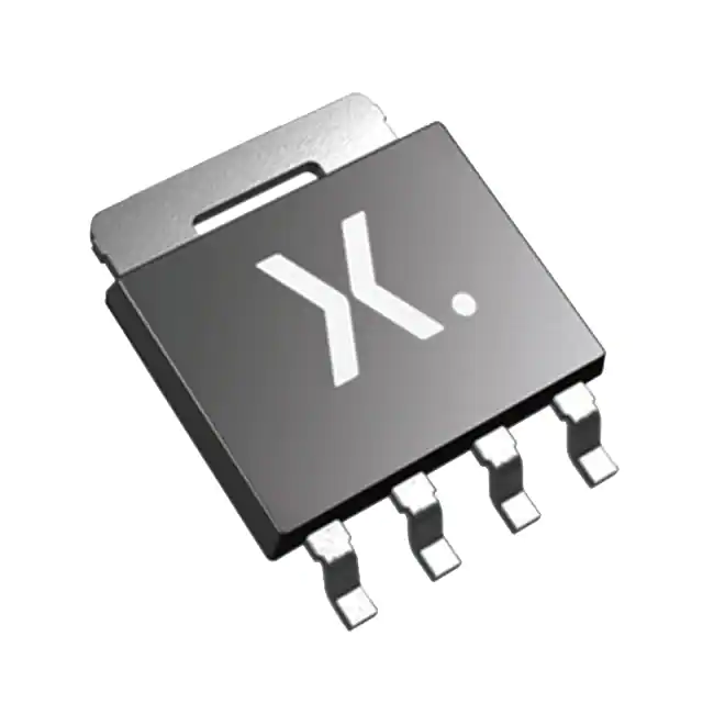
- 封装类型为 SOT669(LFPAK),带有 4 个引脚。


参数特性: - 快速参考数据:包括漏源电压(Vps)、漏电流(lo)、总功耗(Ptot)等。

- 动态特性:包括栅漏电荷(QGD)。

- 静态特性:包括漏源导通电阻(RDSon)。

- 热特性:包括从结到安装基座的热阻(Rth(j-mb))。

- 特性:包括漏源击穿电压(V(BR)DSS)、栅源阈值电压(VGS(th))、漏漏电流(lo)、栅漏电流(IGss)等。


功能详解: - 该器件设计用于 DC-to-DC 转换器、笔记本电脑、便携设备和开关模式电源。

- 包括连续和峰值漏电流与漏源电压的关系图、栅源电压与栅电荷的关系图、输入、输出和反向传输电容与漏源电压的关系图等。


应用信息: - 适用于需要超低电平 FET 的应用,如笔记本电脑、便携设备和开关模式电源。


封装信息: - 封装类型为塑料单端表面贴装包(LFPAK),型号为 SOT669,具有 4 个引脚。


文档还包含了修订历史、法律信息、免责声明和联系信息。
PH2925U,115 价格&库存

很抱歉,暂时无法提供与“PH2925U,115”相匹配的价格&库存,您可以联系我们找货

免费人工找货
PH2925U,115
  •  国内价格 香港价格
  • 1+17.158261+2.22434
  • 10+10.9002310+1.41307
  • 100+7.32455100+0.94953
  • 500+5.79260500+0.75093

库存:2148

PH2925U,115
  •  国内价格 香港价格
  • 1500+5.048711500+0.65450
  • 3000+4.674223000+0.60595
  • 4500+4.483474500+0.58122
  • 7500+4.269177500+0.55344
  • 10500+4.1423110500+0.53700
  • 15000+4.0574915000+0.52600

库存:2148