WST02N20
N-Ch MOSFET
Pin Configuration
Features
•
200V/1.2A,
RDS(ON)= 680mΩ(max.) @ VGS=10V
•
•
•
•
ESD Protection
100% UIS + Rg Tested
Reliable and Rugged
Lead Free and Green Devices Available
(1,2,5,6)
DD DD
(RoHS Compliant)
Applications
(3)G
•
•
DC-DC converter for Networking.
Load switch.
(4)S
N-Channel MOSFET
Absolute Maximum Ratings
Symbol
(TA = 25°C unless otherwise noted)
Parameter
Rating
Unit
Common Ratings
VDSS
Drain-Source Voltage
200
VGSS
Gate-Source Voltage
±25
Maximum Junction Temperature
150
TJ
TSTG
Storage Temperature Range
IS
Diode Continuous Forward Current
ID
Continuous Drain Current
IDM a
PD
EAS
b
b
°C
TA=25°C
1.2
TA=25°C
1.2
TA=70°C
0.96
TA=25°C
4.8
TA=25°C
2.5
TA=70°C
1.6
t ≤ 10s
50
°C/W
Steady State
90
°C/W
Avalanche Current, Single pulse
L=0.5mH
1
A
Avalanche Energy, Single pulse
L=0.5mH
0.25
mJ
Pulsed Drain Current
Maximum Power Dissipation
RθJ A c
IAS
-55 to 150
V
Thermal Resistance-Junction to Ambient
A
A
A
W
Note a:Pulse width limited by max. junction temperature.
Note b:UIS tested and pulse width limited by maximum junction temperature 150oC (initial temperature Tj=25o C).
Note c:Surface mounted on 1in2 pad area.
www.winsok.tw
Page 1
Dec.2014
�WST02N20
N-Ch MOSFET
Electrical Characteristics
Symbol
Parameter
(TA = 25°C unless otherwise noted)
Test Conditions
Min.
Typ.
Max.
Unit
V GS=0V, IDS=250µA
200
-
-
V
V DS=160V, V GS=0V
-
-
1
-
-
30
Static Characteristics
BV DSS
Drain-Source Breakdown Voltage
IDSS
Zero Gate Voltage Drain Current
VGS(th)
IGSS
RDS(ON)
d
TJ=85°C
µA
Gate Threshold Voltage
V DS=V GS, IDS=250µA
3
4
5
V
Gate Leakage Current
V GS=±25V, VDS=0V
-
-
±10
µA
Drain-Source On-state Resistance
V GS=10V, IDS=1A
-
570
680
mΩ
I SD =1A, VGS=0V
-
0.8
1.3
V
-
48
-
ns
-
70
-
nC
-
4
-
Ω
-
280
-
-
25
-
-
8.5
-
-
10
18
-
8
15
-
9
17
-
2
4
-
6
9
-
2
-
-
1.5
-
Diode Characteristics
VSD d
Diode Forward Voltage
trr
Reverse Recovery Time
Qrr
Reverse Recovery Charge
Dynamic Characteristics
e
RG
Gate Resistance
C iss
Input Capacitance
Coss
Output Capacitance
Crss
Reverse Transfer Capacitance
td(O N)
Turn-on Delay Time
tr
Turn-on Rise Time
t d(OFF)
Turn-off Delay Time
tf
V GS=0V,VDS=0V,f=1MHz
V GS=0V,
V DS=30V,
Frequency=1.0MHz
V DD =30V, RL =30Ω,
I DS=1A, VGEN =10V,
R G=6Ω
Turn-off Fall Time
Gate Charge Characteristics
Qg
I SD =1A, dl SD/dt=100A/µs
pF
ns
e
Total Gate Charge
Qgs
Gate-Source Charge
Q gd
Gate-Drain Charge
V DS=100V, V GS=10V,
I DS=1A
nC
Note d:Pulse test ; pulse width≤3 00µs, duty cycle≤2%.
Note e:Guaranteed by design, not subject to production testing.
www.winsok.tw
Page 2
Dec.2014
�WST02N20
N-Ch MOSFET
Typical Operating Characteristics
Power Dissipation
Drain Current
1.4
3.0
1.2
1.0
ID - Drain Current (A)
Ptot - Power (W)
2.5
2.0
1.5
1.0
0.8
0.6
0.4
0.5
0.2
o
o
0.0
T A=25 C,VG=10V
T A=25 C
0
20
0.0
40
60
80
100 120 140 160
20
40
60
80
100 120 140 160
Tj - Junction Temperature (°C)
Tj - Junction Temperature
Safe Operation Area
Thermal Transient Impedance
10
1
300µs
1ms
0.1
10ms
100ms
1s
DC
o
TA=25 C
0.01
0.1
1
10
100
800
Normalized Transient Thermal Resistance
s(o
n)
Lim
it
2
Rd
ID - Drain Current (A)
0
0.2
0.1
0.05
0.02
0.1
0.01
0.01
Single Pulse
2
1E-3
1E-4 1E-3 0.01
VDS - Drain - Source Voltage (V)
www.winsok.tw
Duty = 0.5
1
Mounted on 1in pad
o
RθJA : 50 C/W
0.1
1
10
100 1000
Square Wave Pulse Duration (sec)
Page 3
Dec.2014
�WST02N20
N-Ch MOSFET
Typical Operating Characteristics (Cont.)
Output Characteristics
Drain-Source On Resistance
5
1400
VGS=8,9,10V
1200
RDS(ON) - On - Resistance (mΩ)
4
ID - Drain Current (A)
7V
1000
3
6.5V
2
6V
1
0
5.5V
5V
0
1
2
3
4
800
VGS=10V
600
400
200
0
5
0
1
2
3
VDS - Drain - Source Voltage (V)
ID - Drain Current (A)
Gate-Source On Resistance
Gate Threshold Voltage
IDS=1A
1200
IDS =250µA
Normalized Threshold Voltage
RDS(ON) - On - Resistance (mΩ)
5
1.4
1400
1000
800
600
400
4
5
6
7
8
9
1.0
0.8
0.6
0.4
-50 -25
10
VGS - Gate - Source Voltage (V)
www.winsok.tw
1.2
0
25
50
75 100 125 150
Tj - Junction Temperature (°C)
Page 4
Dec.2014
�WST02N20
N-Ch MOSFET
Typical Operating Characteristics (Cont.)
Source-Drain Diode Forward
Drain-Source On Resistance
5
3.0
VGS = 10V
IDS = 1A
IS - Source Current (A)
Normalized On Resistance
2.5
2.0
1.5
1.0
o
Tj=150 C
1
o
Tj=25 C
0.5
o
RON@Tj=25 C: 580m Ω
0.0
-50 -25
0
25
50
75
0.1
0.0
100 125 150
1.0
1.2
Gate Charge
300
Ciss
250
200
150
100
50
Coss
Crss
8
16
1.4
10
VGS - Gate-source Voltage (V)
C - Capacitance (pF)
0.8
Capacitance
VDS =100V
9
IDS =1A
8
7
6
5
4
3
2
1
24
32
0
40
VDS - Drain-Source Voltage (V)
www.winsok.tw
0.6
VSD - Source - Drain Voltage (V)
Frequency=1MHz
0
0.4
Tj - Junction Temperature (°C)
350
0
0.2
0
1
2
3
4
5
6
QG - Gate Charge (nC)
Page 5
Dec.2014
�WST02N20
N-Ch MOSFET
Package Information
D
e
E
E1
SEE
VIEW A
b
c
0.25
A
A2
e1
L
0
A1
GAUGE PLANE
SEATING PLANE
VIEW A
S
Y
M
B
O
L
A
RECOMMENDED LAND PATTERN
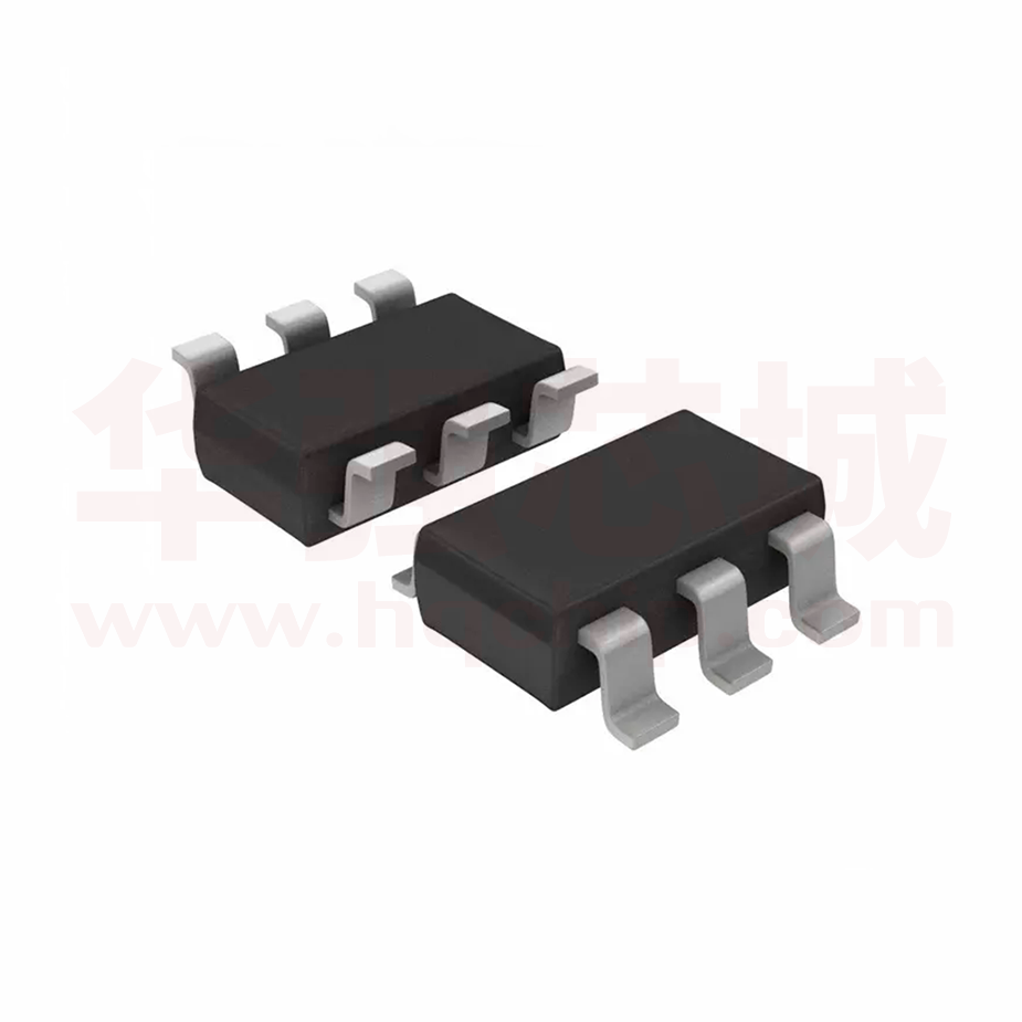
SOT-23-6
MILLIMETERS
INCHES
MAX.
-
0.63
MIN.
MAX.
1.25
-
0.049
0.00
0.05
0.000
0.002
A2
0.90
1.20
0.035
0.047
b
0.30
0.50
0.012
0.020
c
A1
MIN.
0.08
0.22
0.003
0.009
D
2.70
3.10
0.106
0.122
E
2.60
3.00
0.102
0.118
E1
1.40
1.80
0.055
0.071
e
0.95 BSC
e1
2.4
0.8
0.037 BSC
1.90 BSC
0.075 BSC
L
0.30
0.60
0
0°
8°
0.012
0°
0.024
8°
0.95
UNIT: mm
Note : 1. Follow JEDEC TO-178 AB.
2. Dimension D and E1 do not include mold flash, protrusions or
gate burrs. Mold flash, protrusion or gate burrs shall not exceed
10 mil per side.
www.winsok.tw
Page 6
Dec.2014
�WST02N20
N-Ch MOSFET
Classification Profile
www.winsok.tw
Page 7
Dec.2014
�WST02N20
N-Ch MOSFET
Classification Reflow Profiles
Profile Feature
Sn-Pb Eutectic Assembly
Pb-Free Assembly
100 °C
150 °C
60-120 seconds
150 °C
200 °C
60-120 seconds
3 °C/second max.
3°C/second max.
183 °C
60-150 seconds
217 °C
60-150 seconds
See Classification Temp in table 1
See Classification Temp in table 2
Time (tP)** within 5°C of the specified
classification temperature (Tc)
20** seconds
30** seconds
Average ramp-down rate (Tp to Tsmax)
6 °C/second max.
6 °C/second max.
6 minutes max.
8 minutes max.
Preheat & Soak
Temperature min (Tsmin)
Temperature max (Tsmax)
Time (Tsmin to Tsmax) (ts)
Average ramp-up rate
(Tsmax to TP)
Liquidous temperature (TL)
Time at liquidous (tL)
Peak
(Tp)*
package
body
Temperature
Time 25°C to peak temperature
* Tolerance for peak profile Temperature (Tp) is defined as a supplier minimum and a user maximum.
** Tolerance for time at peak profile temperature (tp) is defined as a supplier minimum and a user maximum.
Table 1. SnPb Eutectic Process – Classification Temperatures (Tc)
3
Package
Volume mm
Thickness
很抱歉,暂时无法提供与“WST02N20”相匹配的价格&库存,您可以联系我们找货
免费人工找货- 国内价格
- 5+0.87502
- 50+0.76162
- 150+0.71302
- 500+0.65232
- 3000+0.64530
- 6000+0.62910